The IC designers complete guide to design rule checking
By John Ferguson
Every integrated circuit (IC) designer has a love–hate relationship with design rule checking (DRC). On one hand, it’s the champion that keeps our layouts manufacturable. On the other, it’s the guard that can stall a tapeout hours before deadline with thousands of error markers.
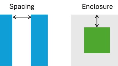
At its core, DRC is the process of verifying that an IC layout complies with the manufacturing constraints defined by the foundry. These “design rules” govern things like minimum metal spacing, via enclosure, poly-to-diffusion overlap and countless other geometric relationships that ensure the chip can actually be fabricated on silicon without catastrophic yield loss.
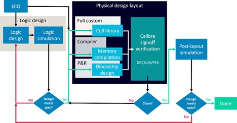
In the broader chip design flow, DRC sits firmly in the sign-off phase—but its influence extends much earlier. Smart teams now push DRC “left” into early design stages to avoid costly surprises later – an approach we like to call shift left verification. Whether you’re a seasoned layout engineer or an EDA student just diving into IC design, understanding DRC is essential.
A brief history of design rule checking
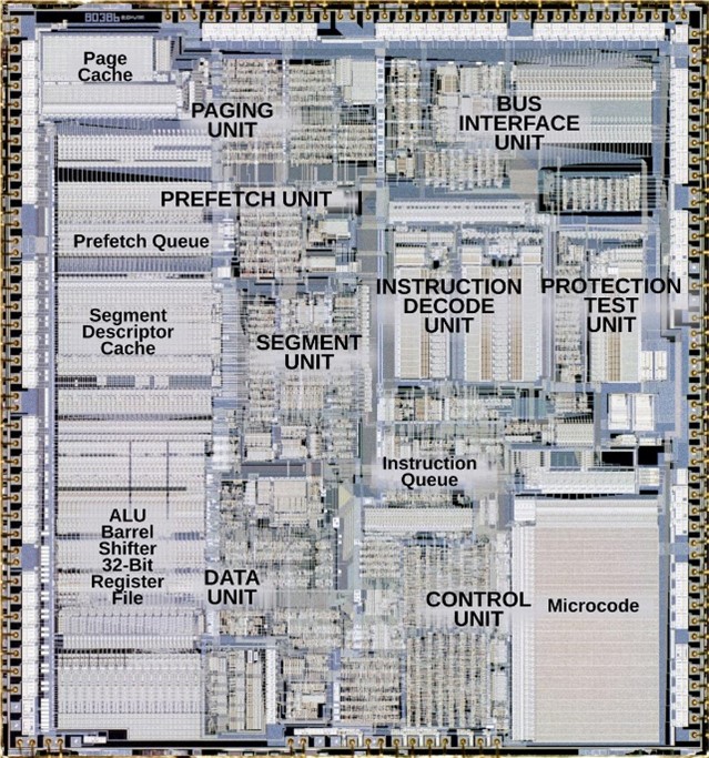
In the early days of IC design (1970s and 1980s), design rules were relatively simple. Foundries defined a set of constraints like metal spacing must be at least 2 microns or poly must overlap diffusion by 0.5 microns. Designers checked these manually—or used rudimentary software tools that flagged obvious violations.
By the late 1980s and early 1990s, as layouts grew in size and complexity, automated rule-based systems became essential. DRC engines evolved to process entire chip layouts, not just small blocks, though rules remained largely geometric and straightforward. The early 2000s marked a turning point. As feature sizes shrank below 130 nm, lithography limits forced the introduction of far more complex rules. Suddenly, spacing wasn’t just about numbers—it depended on context: line-end extensions, neighboring features and orientation all mattered. DRC transformed from a simple checklist into a sophisticated computational geometry problem.
How DRC has changed over time
Shrinking process nodes
With each shrink the manufacturing process node, density and performance doubled as per Moore’s law, but DRC complexity also seemed to double. At 28 nm and below, multi-patterning lithography brought new spacing, coloring and patterning rules. At 7 nm and 5 nm, extreme ultraviolet (EUV) lithography added another layer of nuance.
Beyond rule-based systems
The transition from “simple numbers” to context-aware rules was dramatic. Designers could no longer rely on a single minimum spacing rule—violations might depend on shape orientation, density, or surrounding geometries.
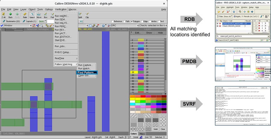
DRC+ and Pattern Matching
To cope, foundries and EDA vendors introduced pattern matching, often branded as DRC+. Rather than encoding every scenario as a rule, foundries provided libraries of problematic geometries. The DRC tool flagged instances of these patterns directly, simplifying rule decks and improving accuracy.
Pattern matching is especially effective for lithography “hotspots”—shapes that technically pass basic rules but fail in printability.
Challenges that have been solved
While you might not hear a lot about advancements in DRC, it has come a long way in making designers’ lives easier:
- Automation of DRC flows
Gone are the days of manual checking. Modern DRC engines can process billions of polygons across hierarchical designs with minimal user intervention. - Hierarchical design rule checks
Instead of flattening a chip layout (which would be computationally impossible at today’s scales), tools now check designs hierarchically—analyzing blocks and sub-blocks in context without exploding data volume. This approach not only saves runtime and memory while preserving accuracy, but also allows massive parallelization across compute clusters.
Modern DRC engines can distribute workloads across hundreds or even thousands of CPUs and multiple servers, enabling performance that scales efficiently well past 1,000 total CPUs for the largest advanced-node processes. This scalability is essential for full-chip signoff at 3 nm and below, where designs routinely exceed billions of polygons. - Foundry-supplied rule decks
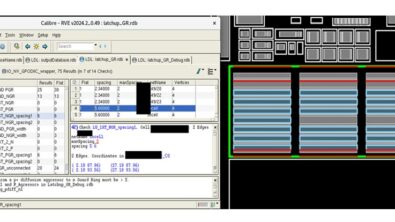
Foundries now make official DRC rule decks available to design teams. These decks encode thousands of process-specific rules in a format optimized for signoff tools like Calibre, which serves as the industry reference standard for accuracy and compliance.
While multiple EDA vendors may support execution of these rule decks, all results are ultimately benchmarked against Calibre’s output to ensure consistency with foundry-certified signoff. This approach provides designers with confidence that their verification results align precisely with manufacturing expectations—regardless of the design environment or flow integration used.
Major milestones in IC design that shaped DRC
The evolution of DRC mirrors the broader milestones in integrated circuit design. Each breakthrough in manufacturing or design methodology forced verification practices to evolve.
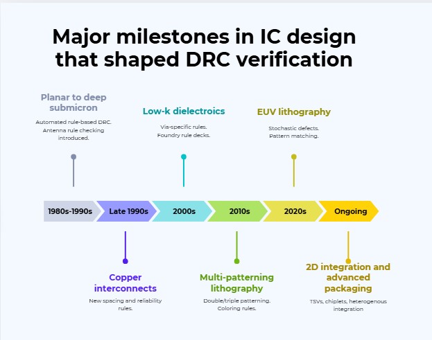
Some highlights:
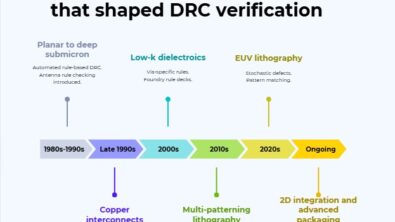
- Planar to deep submicron (1980s–1990s)
As features shrank below one micron, manual checks became infeasible. This era cemented automated rule-based DRC as a permanent fixture in the design flow. It also introduced the need for antenna rule checking, as long interconnects could accumulate charge during fabrication and damage delicate gate oxides. Foundries began specifying antenna ratios and DRC tools added dedicated checks and automated fixes (like diode insertion or metal hopping). - Introduction of copper interconnects (late 1990s)
Replacing aluminum with copper boosted performance but introduced new spacing and reliability rules (such as chemical–mechanical polishing constraints). DRC adapted with more complex enclosure and density checks. - Low-k dielectrics and dual damascene (2000s)
The adoption of low-k dielectrics brought fragility issues, while dual damascene processes added via-specific rules. Hierarchical checking and early foundry rule decks emerged to manage the complexity. - Multi-patterning lithography (2010s)
At 20 nm and below, double- and triple-patterning forced the creation of coloring rules. DRC tools evolved to handle not just geometry, but also mask assignment and decomposition. - Extreme ultraviolet (EUV) lithography (2020s)
EUV relieved some multi-patterning burdens but introduced stochastic defects and new mask rules. Pattern-matching (DRC+) became vital to flag hotspots missed by traditional rules. - 3D integration and advanced packaging (ongoing)
Technologies like TSVs (through-silicon vias), chiplets and heterogeneous integration bring unique cross-die verification challenges. DRC is expanding beyond 2D geometry into the third dimension.
Bonus content on this topic! A comprehensive approach to 3D IC physical verification
Each milestone pushed DRC from simple geometric checks into a far more context-aware, multi-physics discipline. The story of IC design is inseparable from the story of its verification. And just as every new technology node demanded new verification methods, the next wave of innovations will redefine DRC once again.
What’s next for DRC in IC design?
Looking at past milestones gives us a clear lesson: every leap in IC technology requires a leap in verification. If copper, low-k dielectrics and multi-patterning forced new DRC methods, then tomorrow’s challenges—like (gate-all-around) GAA transistors, backside power delivery and chiplet-based systems—will demand even smarter verification strategies.
Here’s where the industry is heading:
- AI/ML in DRC systems
Instead of hardcoding every rule, AI models could predict likely hotspots based on historical data. Just as pattern matching transformed verification in the EUV era, AI may be the defining milestone of the next decade. - Greater context-awareness
Expect DRC to evolve toward intent-based verification—understanding not just geometry, but also designer intent. For example, distinguishing between critical nets and non-critical ones when prioritizing errors. - Standardization of rule decks (SVRF)
While many EDA tools attempt to support various rule formats, the Calibre SVRF (Standard Verification Rule Format) has long been the industry’s trusted and most widely adopted standard for defining design rules.
Foundries worldwide author and distribute their official signoff decks in SVRF syntax because it provides unmatched accuracy, flexibility and reliability across process technologies—from mature planar nodes to the most advanced FinFET and GAA architectures.
SVRF’s rich syntax supports both traditional geometric checks and advanced constructs such as pattern matching, equation-based rules and context-aware verification. It’s the common language of DRC signoff—ensuring that Calibre results are consistently recognized as the golden reference across the entire semiconductor ecosystem.
In short: SVRF isn’t just a format—it’s the backbone of modern signoff verification. Its accuracy and foundry trust continue to shape the evolution of DRC and ensure alignment between design intent and manufacturing reality.
Want a few Calibre-specific updates? Watch this quick video on our website.
Conclusion
Design rule checking has traveled a long road: from simple spacing checks in the 1980s to today’s context-aware, pattern-matching, multi-terabyte sign-off runs. It remains a cornerstone of IC design, evolving alongside every advance in process technology.
The challenges aren’t going away. If anything, the move into 3 nm, 2 nm and GAA architectures will push DRC to new limits. But with advances in AI, standardization and smarter flows, designers can look forward to faster, more accurate checks that align more closely with manufacturing reality.
For IC designers and EDA students alike, mastering DRC isn’t optional—it’s survival. So keep learning, stay close to your foundry’s latest rule decks and explore the latest verification tools.
Key Takeaways
- It is essential for manufacturability
Design rule checking ensures IC layouts comply with foundry rules, preventing yield loss and fabrication failures. - Complexity has grown with smaller nodes
What began as simple spacing rules has evolved into context-aware checks, multi-patterning constraints and lithography hotspot detection. - Automation and foundry decks solved major pain points
Hierarchical checking, automated flows and standardized foundry-supplied decks made DRC scalable for billion-transistor designs. - Challenges persist at advanced nodes
Runtime bottlenecks, false positives and adapting to EUV remain pressing issues for both designers and EDA vendors. - The future of DRC is smarter and earlier
AI/ML, intent-based rules and shift-left verification will make DRC more predictive, more efficient and better aligned with manufacturing realities.
Quick Glossary:
- Design rule checking (DRC): Verification step that ensures IC layouts follow foundry manufacturing rules.
- Antenna effect: Charge accumulation on interconnects during fabrication that can damage gate oxides; addressed with antenna rule checking.
- Pattern Matching: A verification technique that flags problematic geometries based on known “hotspot” patterns, beyond simple spacing rules.
- Hierarchical DRC: A method of checking layouts at multiple design levels to save runtime and memory without flattening the entire chip.
- EUV (extreme ultraviolet) lithography: A next-gen lithography technology for advanced nodes (7 nm and below), which introduces new defect and mask-related challenges.
- Shift left verification: Moving verification steps earlier in the design flow to catch issues sooner and reduce rework.