Shift left for more efficient block design and chip integration
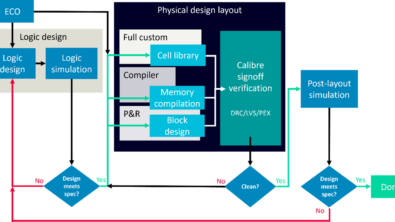
Block/chip integration is a lot more complicated than it gets credit for. On the face of it, chip integration just involves collecting all the IP and other parts, then gluing them all together. In reality, chip integration is an overlapping series of iterations where the pieces that will make up the chip are still being designed, often by multiple different teams. The chip designer is trying to build something that is dependent on those components but can’t wait until all the components are done to start the integration because of time-to-market pressures. That means that the chip designer is doing a lot of iterations with snapshots of IP blocks that are in various states of readiness. When they go through the flow, incomplete blocks will have millions of violations, too many to efficiently review taking a lot of time to debug and fix. How can block/chip integration flows change to be more efficient?
What if some of the time-consuming signoff verification tasks could be done quicker and earlier in the design process? Fix DRC errors with signoff accuracy directly from the place and route tool? Configure and manage all the verification jobs like a world-class maestro?
These are all capabilities available now in Calibre Shift Left tools. The benefits for block design and chip integration teams include:
- Early physical, circuit and reliability verification
- Violation debugging integrated in the design layout environment
- Optimize configuration and management of multiple jobs
For many designers the Calibre tools come to mind as part of sign-off physical, circuit and reliability verification as the designs are nearly clean. For blocks that are not quite complete, full signoff Calibre runs will take a long time and return a huge number of violations so less accurate, but more integrated verification tools may be used in the earlier design stages. New Calibre tools and use models enable a smarter shift-left strategy that brings Calibre-accurate analysis and verification to all the early steps of the block/chip design flow as well. Using the Calibre tools to perform smaller iterations of design steps creates a more efficient flow that saves a lot of time while mitigating risks of significant rework due to less accurate analysis during the design stage.
Early design-stage physical, circuit and reliability verification
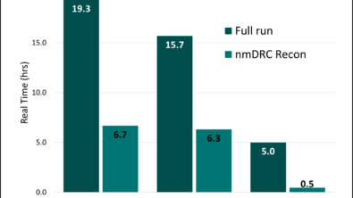
Running the full DRC signoff flow on IP that isn’t complete is inefficient. Instead, designers can use the Calibre nmDRC Recon tool to reduce runtime and focus debugging efforts. It intelligently analyses all the rules in the process design kit (PDK) and identifies which ones would consume massive amounts of processing time given the complexity and types of checks. At the early stages of the block/chip integration, when the design is ‘dirty’, the tool will decide that some checks, like connectivity and density, don’t need to be run yet. The tool automatically selects the optimal set of the most checks that run very fast and give the designers useful information about what needs to be cleaned up first. Compared to a full DRC run, using the Calibre nmDRC Recon tool reduces overall turnaround time as much as 5X (figure 1).
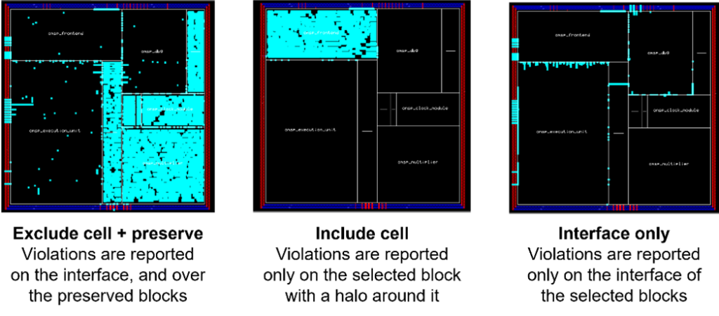
In addition to running only the subset of important and useful checks, designers can also exclude dirty or unfinished blocks from the DRC run to focus on the applicable areas/blocks. Rather than verify the entire layout, you can focus the work on certain areas, like just the top level but exclude unfinished or dirty blocks. The excluded IP or blocks are not treated as black boxes, but as gray boxes so you can still see errors resulting from the interactions between blocks and between IP and the top-level chip (figure 2). By gray boxing some of the layout, the verification runs much faster and finds just the violations that are meaningful in context.
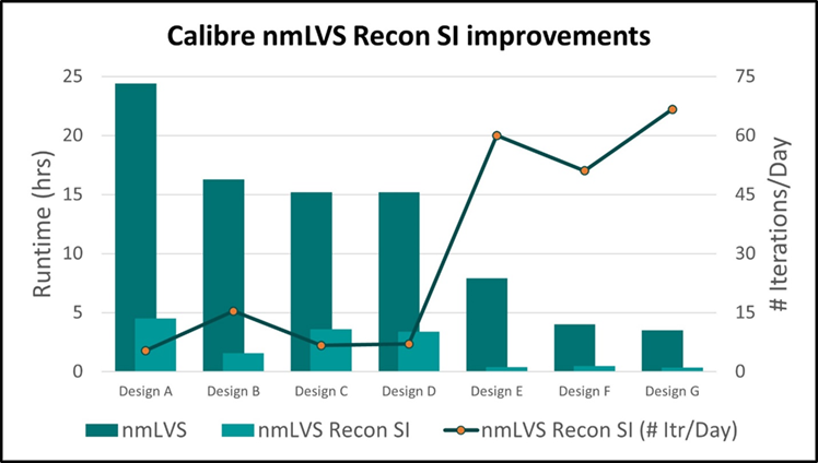
Layout vs. schematic (LVS) checking is made up of several categories of checks, including short isolations, connectivity conflicts, ERC and LVS compare. These checks take a long time even on clean designs; when a design is dirty, the runtime explodes. Calibre nmLVS Recon lets designers run categories of checks individually, so you could independently run just short path isolation checks, for example, without the rest of the LVS tasks and focus on cleaning those up in the early design stages. This partitioned checking requires no editing of the rules deck; the tool automates running the subset of focused checks and saving you orders of magnitude in runtime over running the entire LVS deck. This lets you increase the fix-check iterations by 5X to 65X a day, a giant productivity improvement. (figure 3).
Design optimizations for reliability—like double via insertion, power grid interconnect redundancy, adding decoupling capacitors, doing engineering change orders and filler cell insertion—have traditionally been done in the place and route tools and then checked by Calibre and iterated back to P&R when issues are discovered. New capabilities shift Calibre left into this activity. Calibre DesignEnhancer can now perform those layout modifications with signoff-quality results during IC design implementation. Calibre DesignEnhancer performs these tasks faster than the routing tool can and the results are Calibre clean.
DRC error debugging integrated in the design layout environment
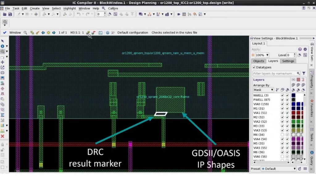
How much time would it save block/chip teams if they could make Calibre signoff-quality layout optimizations within the design implementation tool directly? The Calibre Realtime Digital tool does just that. It enables on-demand Calibre sign-off design rule checking inside the P&R tool, letting physical design and verification engineers optimize their manual DRC fixes and focus on meeting their power, performance and area (PPA) goals in far less time.
From the layout design GUI, when you make a layout change to correct a DRC error, Calibre runs automatically in the background to verify the modifications in the region, so you know immediately if the original violation is fixed and if any new ones were introduced (figure 4). Getting real time information about your edits is far more productive than the traditional flow of making edits, writing out the design, a running another batch verification. Over the life cycle of the design implementation Designers see 40% to 60% savings in time to final signoff closure.
You can read more about Calibre’s shift left for block/chip designers in our technical paper, Navigating design challenges: block/chip design-stage verification.
These Calibre shift-left technologies improve productivity, let you run design-fix iterations faster and shorten time to tapeout. But, it’s not just about improving the efficiency of traditional design activities. Calibre is also building capabilities for analysis and verification of new multiphysics effects seen in advanced process nodes. Multiphysics refers to the combined and intermingled effect on circuits of power, heat, and mechanical stress, and becomes more important for 3D or multi-die designs. These types of verification are new to the industry but are quickly becoming necessary. Being able to incorporate these new checks into your existing Calibre tooling ensures consistent and trustworthy results. The tools for power, thermal and stress analysis and verification also fit into the shift-left strategy, and work throughout the design flow, not just for signoff.
Optimize configuration and management of multiple jobs
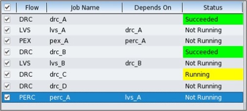
Calibre has also created other new capabilities to help boost efficiency. While reducing the time of doing one verification run is nice, we want to streamline the entire complex workflow. The Calibre Interactive tool lets designers setup and automate a series of tasks through an interactive multi-job manager (figure 5). It automates managing and submitting of multiple jobs and the workflow of which can run in parallel or have series dependencies. This is not only useful for managing a series of DRC/LVS/PEX/PERC runs but is very handy in managing the common practice of splitting the deck into subsets of checks so different runs can run in parallel and focus on different issues.
Another new enhancement available for deck splitting seeks to reduce time spent in Calibre database construction. The first thing Calibre does when running jobs is a database construction step, where it optimizes all the data coming in before it starts executing the checks so that those checks can run with optimal performance and predictability. But running that database construction takes time. So, if you break up the rules deck and execute split runs for several different subsets of rules, Calibre will have to perform database construction for each of those split runs. However, with the new Reusable HDB capability you can run the database construction one time with all the rules turned on and save it to disk. Then the subsequent split jobs will all use that one database and can immediately start executing the checks. This improves throughput and efficiency for all the split runs.
These types of workflow optimizations provide comprehensive improvements to efficiency that save designers time and money when getting chips out to market.