The “next” technology node: ready or not, here it comes
By Shelly Stalnaker
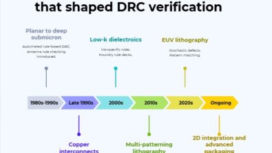
For years, decades even, the semiconductor industry has lived by the process node, which was originally named by its most crucial dimension, the length of the transistor’s gate, which controls the flow of current through the device. Thus, back in the 90’s, you had the 350, 250, and 180nm nodes. The industry broke new territory around 2007, when it introduced the first “deep sub-micron” node at 90nm. Just 13 years later, and 7nm designs are in production, 5nm and 3nm are in development, and 1nm is being researched.
Of course, we all know that those newer designations don’t really, actually, reflect the physical gate length any longer. Today’s terminology is simply a shortcut name that gives a title to a collection of design and manufacturing technologies that distinguish one node from the next. But one thing is clear—integrated circuit (IC) design and manufacturing has changed significantly. Innovations such as immersion lithography, multi-patterning, and finFET transistors (as well as their newer cousins, the gate-all-around finFET and carbon nanosheet transistors) have helped maintain the forward motion of IC technology and functionality. Advances in electronic design automation (EDA) software have, so far, enabled the semiconductor industry to keep producing larger and more complex chip designs in reasonable, although continuously lengthening, time to market schedules. But what happens next?
Quite a lot, as it turns out. In addition to technical innovations in IC design and manufacturing, changes in the semiconductor industry itself are emerging. Those huge and complex designs can now be brought to market faster by making massive amounts of compute resources available in the cloud, opening the market mode widely to companies that would previously have been limited by their ability to acquire the needed physical resources. With the emergence of reliable and accurate verification software, 3D packaging is enabling design companies to more easily and confidently “mix and match” design styles and process nodes to take advantage of both cost-efficient established nodes and “function-forward” advanced nodes in a single computing package.
EDA companies continuously work in collaboration with both design companies and foundries to ensure that what those design companies can dream up can become a physical reality. New approaches such as machine learning and artificial intelligence improve and expand verification and analysis capabilities. Constant engine optimization and “shift left” strategies ensure the most efficient operational environments in the face of increasing resource demands. A focus on ease of use in tool design automates and simplifies many routine tasks, and enables smoother integration between EDA tools from different suppliers.
If you’re interested in exploring any of these topics, here’s a few of our recent white papers that might prove to be informative. Download one, or all, and settle in for a good read.
- New approaches to physical verification closure and cloud computing come to the rescue in the EUV era
- EDA in the cloud—Now more than ever
- Reliability verification in the cloud delivers significant runtime benefits
- Automated ESD protection verification for 2.5D and 3D ICs
- Context-aware SPICE simulation improves the fidelity of ESD analysis
- Automated waiver management for IC reliability verification
- Modeling electrochemical deposition with machine learning for chemical mechanical polishing simulation
- Automated waiver management for IC reliability verification
- Customize and standardize your IC verification configuration