Caution! Avoid detours when improving resistance on ESD paths
By Derong Yan
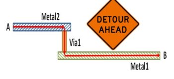
As overall transistor dimensions shrink, integrated circuit (IC) chip designs become more sensitive to the damage caused by electrostatic discharge (ESD). Most semiconductor foundries provide ESD design rules to check for violations that must be fixed before the tapeout of any IC chip design. Some of these ESD design rules require that the resistances along ESD discharge paths must be lower than specified design thresholds. If you find that the resistance of an ESD discharge path exceeds the threshold allowed by the relevant ESD design rule, you’ll have to modify the layout design to reduce the resistance of the ESD path. However, in a large and complex chip design, an ESD discharge path can traverse more than a dozen metal layers in today’s advanced process nodes. So…where in the layout should layout designers look for possible resistance bottlenecks to fix?
In the design community, there are some misconceptions as to what information layout designers should look for when correcting and improving the resistances of ESD discharge paths. For example, some designers immediately look for the shortest resistance path among the many possible routes of an ESD discharge path, believing this path will help them find the resistance bottleneck to fix. Others look to obtain the sum of resistance by metal and via layers, as they believe this information will give them a clue as to which layer contributes the most to the resistance of an ESD discharge path. In reality, based on my experience, these options are all misconceptions that may look intuitively appealing, but are actually without any substance if you perform some analysis of how resistance of an ESD path is actually calculated. Not only will this kind of information NOT help designers find the root cause, but even worse, it may lead them into dead ends and waste their valuable time during tapeout crunches.
There’s good news though. Layout designers don’t have to rely on their own intuition or take shots in the dark anymore. Electronic design automation (EDA) tools are available to help them quickly identify and fix problematic layouts with automated verification and debugging guidance. For example, the Calibre® PERCTM reliability platform, when combined with the Calibre RVETM results viewer and Calibre DESIGNrev layout viewer, enables layout designers to not only automatically check the resistances of ESD discharge paths in an IC layout, but also quickly see a visual representation of both the total effective resistance of an ESD path, and the contribution made by each metal or via polygon to that resistance. This functionality lets layout designers immediately view and identify the resistance bottleneck along an ESD path so they can make smart layout changes, such as widening metal routes or adding additional vias, that reduce the total effective resistance of the ESD path to remain within design limits.
To learn more about what to look for when fixing ESD resistance violations, check out our white paper, Shortest resistance path deception in ESD protection circuit P2P debug.