Using Automated Pattern Matching For SRAM Physical Verification
By Elven Huang, Mentor Graphics
Accurate SRAM IP verification can be tricky, but automated pattern matching can help.

How often have you struggled to verify static random-access memory (SRAM) blocks in your design? And how often, no matter how much time you spend on them, do they end up causing manufacturing issues?
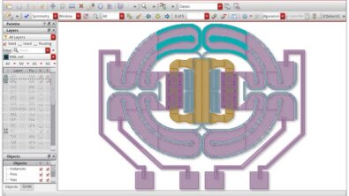
Memory is a critical component in today’s SoC designs, often consuming 50% or more of the die area. SRAM blocks are typically assembled in a layout using a set of specific intellectual property (IP) blocks that abut or overlap one another in a specific arrangement that matches the circuit specifications. Physical verification of SRAM has always been a challenge, because these blocks usually contain smaller feature sizes and spacing constraints compared to traditional logic or other layout structures. At advanced nodes, the smaller process geometries, reduced supply voltages, increasing process variation, and manufacturing uncertainty mean accurate SRAM physical verification results are not only reaching new levels of difficulty, but also new levels of criticality for design success.
Historically, foundries develop SRAM libraries containing IP that are certified for both functionality and a specific process node. Customers then place these SRAM IP in their designs, adjusting as necessary to achieve DRC-clean results. However, any changes a customer makes to these foundry-certified SRAM IP during implementation can impact yield. But foundries provide design rules for SRAM IP to check if any violations occur in placement, don’t they? So why does their use cause so many problems?
The challenge in SRAM physical verification comes from applying a different set of design rules to memory block elements than the rules that apply to the rest of the design, and then catching any unexpected interactions or modified cell elements. Additionally, foundries provide a variety of SRAM types according to their processes, and it is not a simple matter to clearly and accurately describe all their valid usages. SRAM cells involve multiple layers and contain many different geometry shapes with various dimensions, making it nearly impossible to cover all potential placement issues with design rules. For example, can a cell be mirrored, or used with other types of SRAM? In fact, for some floating errors that can only be seen from TOP cell, there is no way to find them with any existing design rule checking (DRC) approaches.
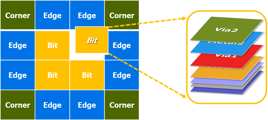
Figure 1: An SRAM block consists of multiple cells, and each cell includes multiple layers.
Prior to 20nm, the manufacturing team could usually make small tweaks during the manufacturing process to avoid or reduce any yield issues they encountered. At 16/14 nm and below, due to the physical limitations of the deep ultraviolet (DUV) lithography process, it is extremely difficult for the manufacturing team to make adjustments, despite the array of tools and techniques they have available, such as multi-patterning, resolution enhancement technology (RET), etc. As a result, design teams are finding it harder and harder to ensure their designs are properly implemented and manufacturable.
The most common solution is to use manual marker layers, which are used by the physical verification rules to identify regions of the design that contain the SRAM, along with “almost” duplicate design rules. Not only does this increase the rule deck complexity, but it also adds the time and burden of supporting these decks in the future. Even more significantly, this approach still can’t detect such issues as IP manipulation, placement overlaps, floating shapes, or unintended interactions (Figure 2).
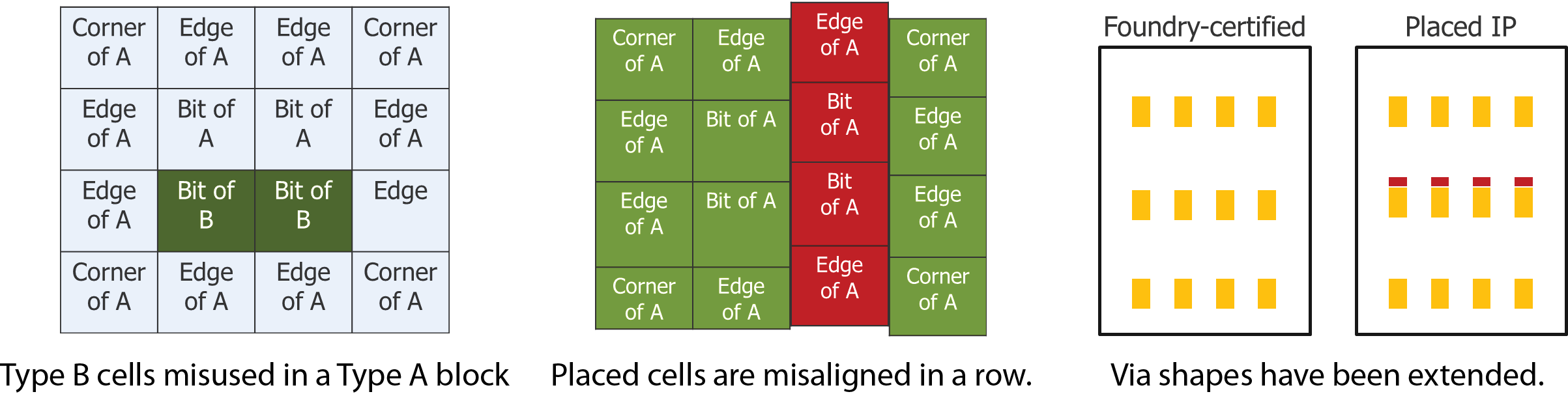
Figure 2: Common SRAM issues that are hard to detect with traditional verification.
The designer is still left pondering… Is the structure assembled properly? Are the proper manufacturing rules being applied to the memory and the rest of the design? Did we miss anything?
Pattern-based SRAM IP validation
Unlike traditional DRC, which is dedicated to one-dimensional checks such as width and space, automated pattern matching can evaluate a pattern consisting of multiple polygon shapes, and check multiple layers. It eliminates the human error inherent in manual marker assignments, and reduces verification time and the expertise needed to write additional design rules. Pattern matching can not only easily and accurately identify IP manipulation and external interactions but also simplify long-term support requirements. Patterns are also easy to update when new IP elements are added.
An automated pattern-based verification flow includes four steps: pattern generation, pattern matching, error identification, and error output (Figure 3).
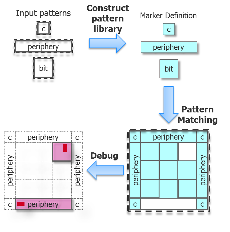
Figure 3: An automated pattern matching process.
Capture elements as patterns
The quality of the patterns in a pattern library determines how well the pattern matching flow can identify violations. Using an assembled SRAM block that includes all of the necessary elements, capture individual cells (such as bitcell (core), edge, top, bottom, corner, etc.) and add them to the pattern library. At a high level, the process is to convert all standard cells to patterns. Ideally, all patterns should abut each other (like the placements in the SRAM block) without overlap. These patterns contain multiple layers, and should be generated from the TOP level to enable floating error checks.
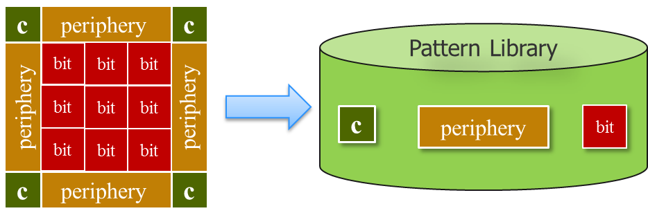
Figure 4: Each part of the SRAM IP is converted to a pattern and stored in the pattern library.
Compile the patterns and test them against an assembled memory structure. Remember that the pattern matching process must find not only the patterns that match, but also any geometries that do not match the intended/required geometry (which can indicate IP modification). Regions not covered by a matched pattern may be due to a valid cell pattern that was not captured, or a contextual interaction that may be acceptable. Contextual interactions in the assembly can cause placed cells to fail to match the pattern due to interactions (Figure 5). If these interactions are acceptable and expected, a new pattern capturing the element in context should be added to the library. Any remaining output error results are real violations that require further analysis by a layout designer to understand why the pattern failed to match. Continue adding patterns and checking until every part of the entire memory structure matches a pattern.
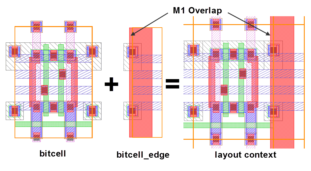
Figure 5: Unexpected contextual interaction.
Once the SRAM pattern library is established and verified, it can be used in your physical verification flow to automatically validate all SRAM IP placements, ensuring that the SRAM IP are both unmodified, and properly implemented in your layout. If new SRAM IP are supplied by the foundry, you simply generate any new patterns needed and add them to your pattern library.
With its powerful ability to capture complex pattern relationships simply and quickly, automated pattern matching enables designers to find and debug difficult SRAM implementation issues and to detect prohibited SRAM IP modification. If you are not already using pattern matching for your advanced node designs, you are missing out on a highly effective technology that can help you bring better designs to market faster.
Author
Elven Huang is a technical marketing engineer supporting Calibre DRC tools and technologies in Mentor Graphics’ Design To Silicon Division.

Liked this article? Then try this –
Blog: How to Use Pattern Matching to Improve Automatic Waiver Management
This article was originally published on www.semiengineering.com