Are You (Really) Ready for Your Next Node?
By Michael White, Mentor Graphics
Skipping nodes is gaining popularity, but it can bring some unexpected challenges. Are you prepared?
The transistor scaling that has been the engine of our industry for 30+ years continues to relentlessly march forward. We are now about to begin production on the industry’s third multi-patterning node—7 nm.
One of the most interesting trends I’m observing is the number of companies choosing to jump a technology node. Of those opting to go that route, skipping to 7 nm seems particularly popular. Skipping any node brings some real challenges, including some that aren’t always recognized or planned on.
The Computational Explosion
Physical verification (i.e., design rule checking, or DRC) just keeps getting harder and harder, whether you’re jumping from 65 nm to 28 nm, or the scariest leap—from 28 nm to 16/14 or 7 nm. Stuck with 193-nm lithography for at least 18 more months (best case), foundries have had no choice but to add more design rule checks to ensure manufacturability at these nodes.
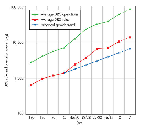
The figure shows us that since 40 nm, the industry has, on average, been increasing check count by 20-30% every node. Similarly, the complexity of each check also is increasing node over node in concert with the growing complexity of the process. For 20 nm and below, multi-patterning techniques have been essential in enabling the industry to continue to progress along Moore’s law for transistor scaling. However, their use also means significant additional computation.
From a foundry deck perspective alone, one must account and plan for a huge computation increase. This is especially the case for those considering jumping more than one node (e.g., 65 nm to 28 nm = 3.2X; 28n m to 16/14 nm = 1.6X; 28 nm to 7 nm = 3.6X).
For very sound manufacturing reasons (to minimize design variability) at the 32/28-nm node, the foundries transitioned from minimizing the number of inserted fill shapes to maximizing the use of fill shapes. At 10 nm and below, these fill shapes are now also being placed at the single mask spacing constraint. Both of these trends have put significant additional computation demand on both the generation and physical verification of DRC-clean fill.
The entire purpose of pursuing Moore’s law for transistor scaling is to deliver more transistors per unit area over time. As an industry, we have been delivering approximately 2X more transistors per technology node, enabling all of the IC-based products our society relies upon. Of course, 2X more transistors per technology also means additional computation effort at each technology node.
IP Complexity
The growth in computational effort isn’t limited to block and full chip implementation and verification. Where historically it was common for custom and intellectual-property (IP) designers to run DRC and other verification tools on single CPUs, now it’s common to run on four CPUs or more.
Growth in the effort per design team isn’t just limited to computation: With ever-increasing complex designs, the number of designers needed per design project expands when moving to advanced nodes for both analog/custom and digital implementation. In analog/custom designs, I’ve seen this staffing need being driven by the rapidly growing number of analog and mixed-signal blocks in a design, an increasing number of complex circuits in nm-node analog, more power-saving modes, etc. Over the last five years or so, it hasn’t been uncommon to hear of 50% node-over-node IP designer staffing increases.
Technical
There are so many new and evolving techniques at leading-edge nodes (e.g., multi-patterning, advanced fill, design for manufacturing, etc.) that I think I’ll save them for a more detailed discussion in another article. Suffice to say that the changes are not only numerous, but challenging to implement.

Where Companies Aren’t Getting it Quite Right
Lack of proper and timely preparation to manage the increase in computation requirements is an issue we’re seeing with more companies than would be expected. For quite a few of these firms, we have heard things along the lines of “back in the day, we didn’t need to add more resources when jumping to a new node and we still had reasonable DRC, etc. run times—so we didn’t budget for more resources,” or “My annual budget increase is 10%, so that is all we have.” For advanced nodes, and certainly for a node jump, under-investing in computing resources simply results in slower design turns and a longer schedule to market.
Staffing at a rate that can keep up with the increased design effort is another challenge, to be sure. In quite a number of cases, the need for additional headcount is understood. Often, though, a smaller-than-needed staff increase is added, or the staffing ramp is started later than needed to bring in a full team and on-board them to the point where they are firing on all cylinders.
Technical training has been an occasional problem, but most of the companies who reach out to their EDA supplier will get the help they need. The two issues above are the dominant problems we see with many across the industry.
What to Do?
First, think long and hard about skipping nodes. Yes, certain market situations may dictate that a company must skip a node to try and catch up with its competitors. But if there’s any reasonable ability to continue the normal progression, do so. There is so much progressive learning node over node now, and the need for this learning doesn’t go away with a node jump. You’ll just end up compressing that learning into the critical path of your next design, while management still expects you to complete that design with the same or shorter schedule as the last one. This can only end in tears.
The idea that a design team can get away with the same compute resources as they had for their last design (or some small percent increase) is a pipe dream. This is especially true with a node jump. Industry-leading tools like Mentor Graphics’ Calibre nmDRC and Calibre nmLVS platforms continuously improve the speed of their engines, and partner with the foundries to optimize the foundry-written decks. However, with the exponential node-over-node increase in compute demands, the use of scaling (more resources) is the only remaining means to maintain constant turnaround time.
Collaborate with your EDA partner early to accurately forecast what your compute resources will need to be for that next design. Use this data to justify to management the investment level that’s really required to meet cycle-time goals.
Talk with your peer companies, IP providers, etc., to realistically plan for the right staffing level required with the more complex IP needed at that next node. Adequate staffing is especially critical if a node jump is mandated. Consider expanding your use of third-party IP or IP design services as a way to “flex up” in both capacity and next-node technical expertise. This is an option I’m seeing used more and more often, and it’s why we’re seeing a large number of IP companies working on multi-patterning node IP.
Using the EDA tools involved in developing the foundry’s process can be extremely helpful. Because that EDA company helped develop the process with the foundry, it has a great deal of valuable experience in what will be needed to be successful at that node, and how you can avoid some of the largest obstacles.
If your company is like mine, it’s now at the beginning of a new strategic planning cycle. Start planning upfront for all your compute and staffing needs that will help ensure a design implementation and verification cycle time that can successfully hit your next market window. Half measures and partial investment will result in late design tapeouts. It’s one of those “you get what you pay for” scenarios. By planning early and realistically, you have a better chance of getting the budget approval for the needed investment, compared to trying to shoehorn in the additional resources and staff you will ultimately ask for after the fact.
Liked this article? Then try this –
Blog: Synthesis of Design Rules and Patterns
This article was originally published on www.electronicdesign.com


