Pattern Matching in Design Verification
By Michael White, Mentor Graphics
Automated pattern matching can solve a wide range of design verification issues. Are you in the loop?

Pattern matching (PM) was first introduced as the semiconductor industry began to shift from simple one-dimensional rule checks to the two-dimensional checks required by sub-resolution lithography. These rule checks proved far more complex to write, hard to code for fast runtimes, and difficult to debug. Incorporating an automated visual capture and compare process enabled designers to define these geometries as layout patterns that could be stored in libraries, re-used in multiple design layouts, and carried forward from one process node to the next.
We are now seeing a rapid proliferation and expansion of pattern matching usage in a range of applications in the design, manufacturing and wafer test domains, across all process nodes. The reasons for this rapid proliferation are two-fold. First, pattern matching’s ability to easily describe very complex relationships between geometries across multiple layers simultaneously allows it to efficiently and accurately find interesting parts of a design. Verification speed and accuracy are ever-growing needs as we continue to extend 193nm lithography, and where historically one-dimensional checks were sufficient, now in-context shapes are the critical elements (Figure 1).
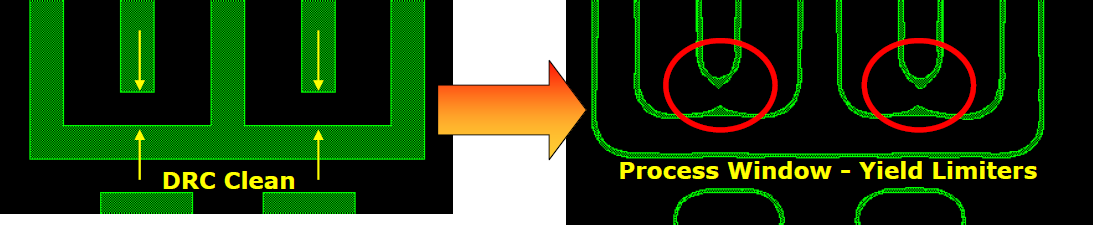
Figure 1. In sub-wavelength lithography, design rule compliance no longer guarantees yield. (Image courtesy of Luigi Capodieci, Ph.D., SPIE Microlithography 2006)
Second, pattern matching’s true power is on display when it is integrated with other physical verification analysis or design tools. Why? Combining pattern matching with traditional design and verification tools enables design and verification engineers to use an automated process to find areas of interest, then make design modifications to fix or waive errors, strengthen the layout against manufacturing defects, etc. This integration and automation has enabled the industry to create a breadth of new pattern matching applications that are achieving results that simply weren’t possible previously.
Let’s explore some of these extended uses. These examples are based on the tight integration of the Calibre Pattern Matching tool with the verification tools that comprise the Calibre nmPlatform solution, which allows for seamless interaction and data access. Processes and results may vary for other pattern matching tools, depending on the degree to which they are integrated with their respective verification environments.
Waiving by Pattern
During design implementation, design rule checking (DRC) errors must be reviewed and fixed in multiple physical verification iterations before proceeding to the parasitic extraction and analysis phases. This iterative process applies to both custom IP design and place and route (or other automated design implementation flows), at any technology node. It is common to “waive” (ignore) DRC errors reported by the sign-off DRC deck or recommended rules deck that are known to actually be manufacturable due to prior design success, simulation or mutual agreement with the foundry. Waivers of tens to thousands of results are not uncommon, and without automatic waving flows, designers can waste days reviewing known-good results over and over in each iteration.
Waivers in intellectual property (IP) blocks are typically identified after physical implementation of the block is completed. The layouts (with their waivers) can then be used in subsequent block or full-chip design implementation. Layout iterations performed at this level can introduce waive-able DRC violations based on the current geometric interactions created by a place and route application or a physical designer. However, the number and location of these contextual waive-able violations may change during subsequent layout iterations, so waiving results does not reduce overall debug time.
Capturing these IP block waivers as patterns that can be dynamically identified with each iteration during physical verification enables automatic waiving of these context-dependent results wherever they may occur as the design topology changes (Figure 2). This waiver methodology can be integrated with traditional IP waiver flows, and can improve designer productivity by focusing debug efforts on fixing real errors, rather than contextual results that may recur throughout design implementation.
Pattern-based waiving is an accurate and effective addition to an automated waiver flow.
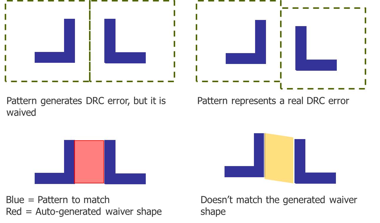
Figure 2. Define contextual patterns and output a waiver database for automated contextual waiving during iterative physical verification runs.
Design Enhancement/Manufacturing Retargeting
Managing systematic defects that occur in the manufacturing process, such as end-of-line via metallization overlap, became a design requirement at 90nm, and continues through later technologies. Yield can be improved by increasing the line extension beyond the minimum value, minimizing the risk of improperly formed vias. Adding line-end extensions to an existing layout first requires an analysis of legal locations for extensions, followed by a re-verification of the design to ensure no design rules are violated. However, defining legal line-end extension locations can require a significant level of coding expertise, which can increase both deck complexity and support challenges, especially if additional requirements must be added later.
A pattern-based approach can be used to capture contextual line ends as patterns, graphically edit the pattern to include the required spacing, and output this data to standard industry formats like GDS or OASIS (Figure 3). Using a graphical interface to identify the patterns in an existing context significantly simplifies the level and amount of coding required. Also, because it is not tied to a specific place and route or other layout implementation tool, a pattern-based approach can be more easily updated as additional contexts are identified.
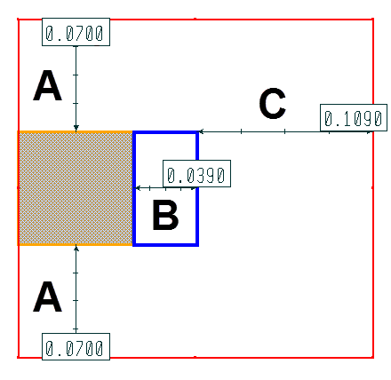
Figure 3. Edit the captured line-end pattern, including any DRC spacing required to ensure a DRC-clean layout.
Complex Device and Curved Layout Verification
It is common for analog and radio frequency (RF) designs, microelectromechanical (MEM) devices, high power ICs, etc. to be composed of curves or other non-Manhattan geometries, which can be challenging to validate in gridded design database formats. Precise multi-segmented polygons forming curves and other shapes can snap during layout verification as a result of layout magnification, layer derivations, or data tiling. Use of traditional one-dimensional DRC checks on such complex structures is generally impractical, as they result in large numbers of false DRC results. Attempts to add these complex devices to an existing rule deck can require major edits, or be outright impossible, when using traditional EDA tools with very limited ability to handle the curved structures common in these designs and devices. Until recently, it was common for designers to “black-box” (ignore) these design areas, manually checking these layouts instead. Such approaches are risky and impractical with more and more of this type of design content contained in advanced system-on-chips (SoCs) found in today’s smartphones, tablets, cars, etc.
Creating a pattern-based validation flow for complex layouts and devices improves verification accuracy dramatically, as well as simplifying the implementation requirements and downstream supportability efforts. Shapes comprising a complex device in advanced RF, MEMs, high power, etc. typically include Manhattan and non-Manhattan polygons. Designers can define a pattern that uses the Manhattan shapes as an anchor layer for pattern recognition, and output the non-Manhattan shapes as a derived layer when the anchor shapes are matched and compared against the non-Manhattan shapes in the original layout (Figure 4). Creating a validation flow using pattern recognition for the device recognition, and simple Boolean operations to output any mismatched device results, ensures that these complex devices can be verified accurately, and in a timely manner.
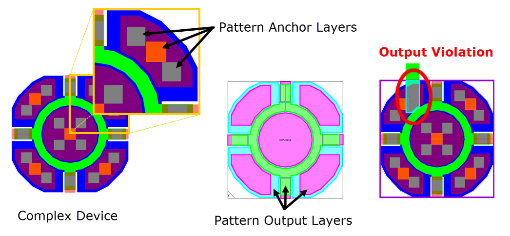
Figure 4. Complex device recognition with pattern anchors can output multiple layers that are used to identify specific violations that require fixing.
In this process, tight integration between pattern matching and DRC is essential to enabling this new, previously impossible type of automated verification.
Yield Detractor Removal
A yield detractor is a shape (or a group of shapes) in the design layout that has been shown to be a systematic (non-random) source of chip failures during manufacturing. Yield detractor geometries result from many manufacturing issues, including lithography and etching characteristics. At 28nm and below, many leading foundries provide yield detractor decks to their customers that consist of “forbidden” patterns defining these specific geometries. These yield detractor pattern libraries are used to identify weak (or “suspect”) patterns in the designs that are in progress, so these patterns can be removed before the design is completed (Figure 5).
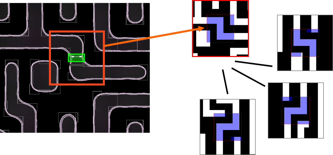
Figure 5. Patterns enable the quick identification and removal of yield detractor geometries in a layout.
In parallel with the growing use of yield detractor pattern libraries by the foundries, fabless companies are identifying their own yield detractor patterns, based on issues from prior designs. Application of this knowledge is sometimes driven by a joint quality process with their foundry, and sometimes by the fabless company’s own unique design methodologies. When fabless companies identify these patterns internally, and maintain the growing pattern library as proprietary information, they can create a significant competitive differentiator. They are potentially able to avoid re-spins, ramp to volume faster, and reduce design variability for their unique design styles.
Foundries and fabless companies have implemented a wide variety of yield detractor solutions, ranging from simply highlighting yield detractor pattern matches, to displaying a pattern-specific fix via the pattern error marker, to enabling automated pattern-matching-driven design fixes.
Summary
We are seeing a rapid proliferation of the use of pattern matching technology across a range of applications and process nodes in the design, manufacturing and wafer test domains. One of the critical benefits driving this explosion is pattern matching’s ability to quickly and accurately filter down to key areas in a design where other verification and analysis tools can then be used to perform a variety of design correction and enhancement actions. The combination and integration of pattern matching with these verification functions enable both the ability to more easily solve hard problems across a broad range of established and advanced technology nodes, and the opportunity to solve design and verification issues that were previously intractable to automated solutions. We expect this expansion of pattern matching applications to continue as more and more people understand its potential and its power.
Author
Michael White is the director of product marketing for Calibre Physical Verification products at Mentor Graphics.

This article was originally published on www.semiengineering.com