Reducing Post-Placement Leakage with Stress-Enhanced Fill Cells
By Valeriy Sukharev, Jun-Ho Choy, Armen Kteyan and Henrik Hovsepyan, Mentor Graphics
Optimizing power usage for mobile devices at advanced nodes is tough. Stress-enhanced fill cells can help.

As downward scaling of transistors continues, optimizing power consumption for mobile devices is a major concern. Power consumption consists of two components: dynamic and static. Dynamic (active) power is used while the chip is performing various functions, while static (leakage) power is consumed by leakage current (Figure 1). For both high-performance and low-cost mobile devices developed with deep sub-micron technology, static power has become the major source of total power consumption, primarily due to the transistor’s off-state sub-threshold leakage current (I^sub). Designers are facing an increased challenge in meeting strict I^sub targets, as scaling transistor threshold voltage (Vt) causes an increase in the sub-threshold leakage current. As a dominant off-state leakage component, reducing I^sub power dissipation has been the subject of numerous research activities.
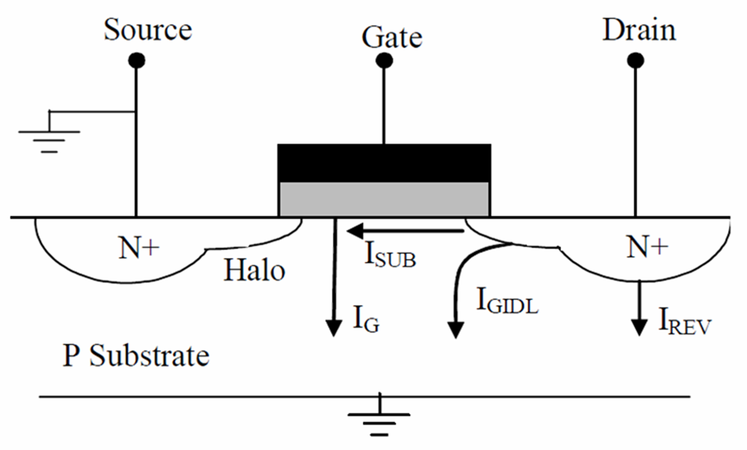
Figure 1. Leakage current components in an NMOS transistor.
A new post-placement simulation methodology and flow using stress-enhanced fill (SEF) cells reduces I^sub by introducing mechanical stress in the device’s channel region. The technique is layout-dependent, provides fine control over Vt, and can be used either independently, or in addition to other techniques.
Leakage Reduction Methodologies
There are two major leakage reduction techniques currently in use: circuit-based and process-based. The circuit-based technique uses transistor stacking, or multi-threshold voltages. One popular method is a dual-threshold CMOS that uses high-threshold voltage transistors on non-critical paths to reduce leakage power, and low-threshold transistors on critical paths to maintain circuit performance. Although this technique can be quite effective in reducing sub-threshold leakage (because I^sub is an exponential function of Vt), it adds significant complexity to the process because it requires additional mask steps.
The process-based technique controls the physical dimensions of device components, such as diffusion length or oxide thickness. One well-known method, strain engineering, introduces mechanical stress in the device’s channel and source/drain regions during device fabrication. Mechanical stress contributes to I^sub in two ways:
- Stress in the transistor region during device fabrication affects the diffusion of pocket ion implants, consequently changing the Vt of MOSFETs.
- Introduced stress in the channel region affects carrier mobility, and controls I^sub, because there is a linear dependence between the two factors.
New capabilities in design verification tools now enable designers to perform stress assessment in stacked 3D-IC chips, as well as analyze the layout-induced transistor-to-transistor stress variation generated by various strain-engineered sources. These sources include contact etch stop layers (CESL), a variety of stress memorization techniques (SMT), and shallow trench isolation (STI) regions. The physics-based compact model employed enables designers to account for both mobility and Vt modifications caused by stress sources. Using such layout stress analysis functionality, we developed and implemented a post-placement simulation algorithm and flow to reduce the off-state leakage current of MOSFET devices.
Any desired stress modifications introduced for leakage optimization must not deteriorate the device’s performance. We determined that modification of STI-induced stress is a feasible way to influence transistor threshold voltage. Due to process-induced impact on the dopant diffusivity, this stress source can have a significant impact on threshold voltage, while its impact on charge carrier mobility may be weaker, due to the larger contribution from intentional stress sources.
Stress for STI is dependent on the length of the active area, as well as the distance between adjacent active devices, which is commonly called STI width (STIW), as shown in Figure 2. This dependency led us to the realization that we could modify the stress by the use of stress-engineered fill cells. In modern standard cell designs, fill cells occupy up to 30% of the total chip area. Because fill cells do not have any functionality, they can be used to generate a desired amount of mechanical stress in neighboring transistor channels. Each fill cell contains “dummy” transistor structures that can be modified to affect the stress in its “neighborhood” without impacting design uniformity. To minimize layout modifications, we performed leakage power reductions only for the pMOS devices with the greatest leakage.
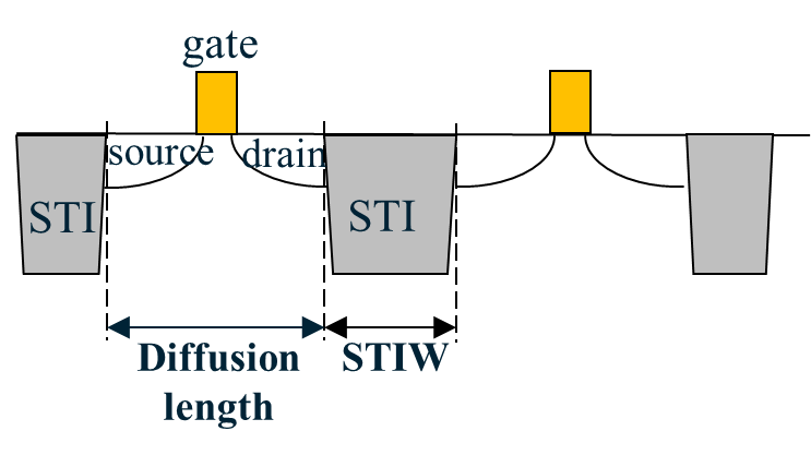
Figure 2. The length of the active area is combined with the STI width (STIW) to determine STI stress.
The main steps of the leakage reduction flow for a given manufacturing process and standard cell library are:
- Design special stress-enhanced fill (SEF) cells that reduce leakage current of neighboring transistors by altering mechanical stress,
- Develop a post-placement optimization algorithm that makes local changes to initial placement and inserts SEF cells in a way that maximizes leakage reduction.
The SEF cell is generated by modifying the “dummy” device layers of standard fill cells. The calibrated stress model demonstrates that Vt of p-type devices can be increased by introducing an STI-induced compressive stress. This effect comes from a p-transistor’s Vt dependency on STIW. We modified the original fill cell by removing active area from the n-well region (Figure 3). This removal increases the amount of STI surrounding the pMOS devices located in adjacent cells, which causes additional compressive stress generation and results in Vt increase in these devices.
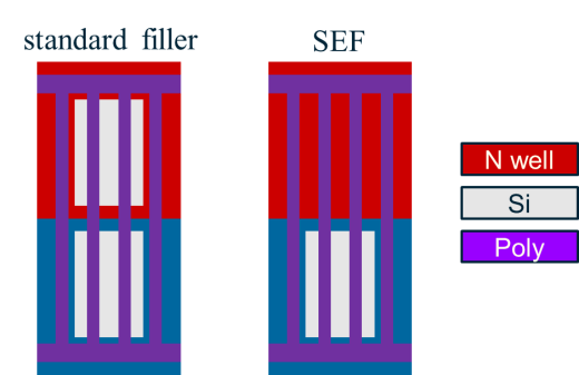
Figure 3. Removing the active area from an n-well region increases the amount of STI surrounding nearby pMOS devices, generating additional stress on these devices.
SEF cell-induced increase in Vt of the pMOS devices depends on a distance between the channel and SEF edges (Figure 4). Insertion of larger SEF cells (containing five and more poly lines) might result in larger Vt changes in individual transistors; however, the net effect can be smaller, due to space limitation for the large SEF insertion.
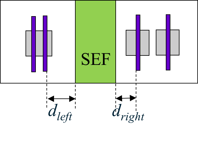
Figure 4. The increase in Vt caused by the SEF cell depends on the distance between the channel and SEF edges.
Placement Optimization Flow
The optimization flow begins by identifying the devices with the greatest leakage. Most leaking devices can be identified with stress assessment models, which must be calibrated for the foundry and technology node used for the chip. For a given foundry process, such a model can:
- Analyze layout-induced stress,
- Identify all stress sources,
- For each device, calculate the change in Vt caused by stress
Cells containing devices with the largest decreases in Vt are considered leakage hotspots. The main constraint in the placement optimization flow is ensuring the locations of pre-defined cells (e.g. clock cells) are unchanged. The key objective in the placement optimization flow is the so-called “optimization zone,” which is defined as a portion of standard cell row between two consecutive fixed cells, as shown in Figure 5. Each zone contains one or more hotspot cells. All optimizations should be done for each zone independently, using a full-featured place and route tool.

Figure 5. The optimization zone is the portion of a standard cell row between two consecutive fixed cells where SEF cells can be inserted.
During the pre-processing step, all standard fill cells are removed to generate free space for the SEF cells insertion. To enable SEF cells insertion in required positions, the optimization algorithm shifts standard cells to the right or left from their original positions within the optimization zone, keeping the order of cells unchanged to reduce possible negative impact on routability. The optimal SEF placement is the one which provides the largest reduction of I^sub within each zone.
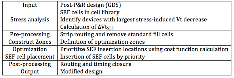
The leakage reduction for an entire cell is the sum of ∆I^sub, calculated for all devices contained in a cell. The optimization algorithm uses this calculation as a cost function to prioritize the locations for SEF insertions so as to produce the largest sub-threshold current reduction. A description of these placement decisions is given below, with a summary shown in Table 1.
- The targeted standard cell block was first placed and routed to completion, then further timing-closed to achieve the targeted performance. Lowest-possible leakage power was achieved using standard techniques, such as Vt-swapping. After stripping off the routing, the completed database was modified as follows.
- A stress assessment model was employed to identify hotspot cells that contain the most leaking devices.
- Standard fill cells were removed.
- In the standard cell rows, the “optimization zones” (representing portions of the row located between two consecutive fixed cells) were defined.
- In each zone, SEF insertion locations were prioritized using the leakage reduction calculation as a cost function, and then SEF insertions were performed according to the priorities.
- Standard-cell block was re-routed using standard place-and-route tool. Block timing was verified again.
- Total leakage in the design with post-optimized layout was re-calculated.
Table 1. Optimization Flow
We performed this optimization simulation on a block of a 28nm technology node design containing ~480,000 cells. After optimization, the number of SEF Cells was ~35,000, which occupied roughly 19% of the total area. The maximum and average optimization zone lengths were 30 and 15 µm, respectively.
Figure 6 demonstrates statistics of the cell shift within an optimized block. 60% of the cells had a displacement of less than 1µm, and the maximum displacement was about 4µm. This minimal displacement significantly helps to maintain the timing closure achieved through placement and routing.
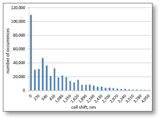
Figure 6. Cell shifts within optimized design blocks.
Figure 7 compares the leakages of the original and modified blocks for a subset of 200 standard pMOS transistors demonstrating the largest change in . On the horizontal axis, these transistors are sorted on the order of decreasing , which is, in general, consistent with decreasing transistor speed. For each block, a line represents the curve fit with exponential function.
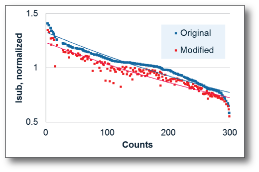
Figure 7. Leakage comparison for a subset of transistors in the original and modified blocks.
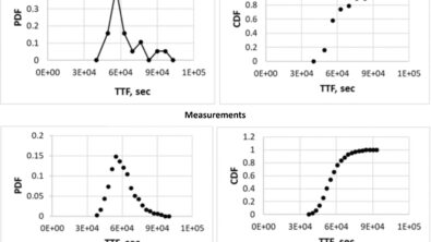
After the test chip was processed on silicon, measurements were done for confirmation of the results. The 28nm test chip was taped out in two versions—an “original” version of the block with the original layout design, and a “modified” version, where the layout was modified using SEFs and the placement optimization flow. Both versions were placed in the same reticle field in close proximity to each other at the time of tape-out, so that any variation in process would be reflected equally in both versions of the block. Power for the targeted block was implemented using a dedicated power supply so there would be no measurement “contamination” from other circuits on the same die.
Figure 8 highlights the results of leakage measurements performed on original and the stress-engineered blocks for various die processed over a range of process conditions. The data show that conservatively, a leakage savings of at least 10% is achieved as a result of optimized SEF cells placement. Timing reports on 1000 worst case slack values for each block show that there is 50ps difference (based on cycle time 1.8ns) between the original and modified blocks. The negative slack is only found for a handful of paths, and can be readily recovered.
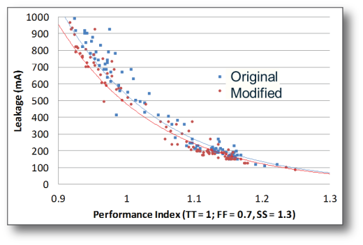
Figure 8. Comparison of leakage measurements performed on original and the stress-engineered blocks for various die processed over a range of process conditions.
Summary
The use of SEF cells can effectively reduce sub-threshold leakage with minimal impacts on chip layouts. Measurements performed on silicon test chips confirmed the predicted leakage reduction of 10-15 percent, while maintaining the same electrical performance. While our research was conducted on standard cells, it is likely that even more benefit can be gained from using this technique on low-Vt and ultra-low-Vt transistors. It should be noted that, for broad adoption, a stress model calibration must be performed for each foundry and every technology node used for chip manufacturing. However, our strain engineering technique is layout-dependent, provides fine control over Vt, and can be used either independently, or in addition to other techniques.

This article was originally published on www.semiengineering.com