A novel methodology for EM assessment in on-power grids can improve power, time-to-market, and design cost
By Valeriy Sukharev, Armen Kteyan, Jun-Ho Choy
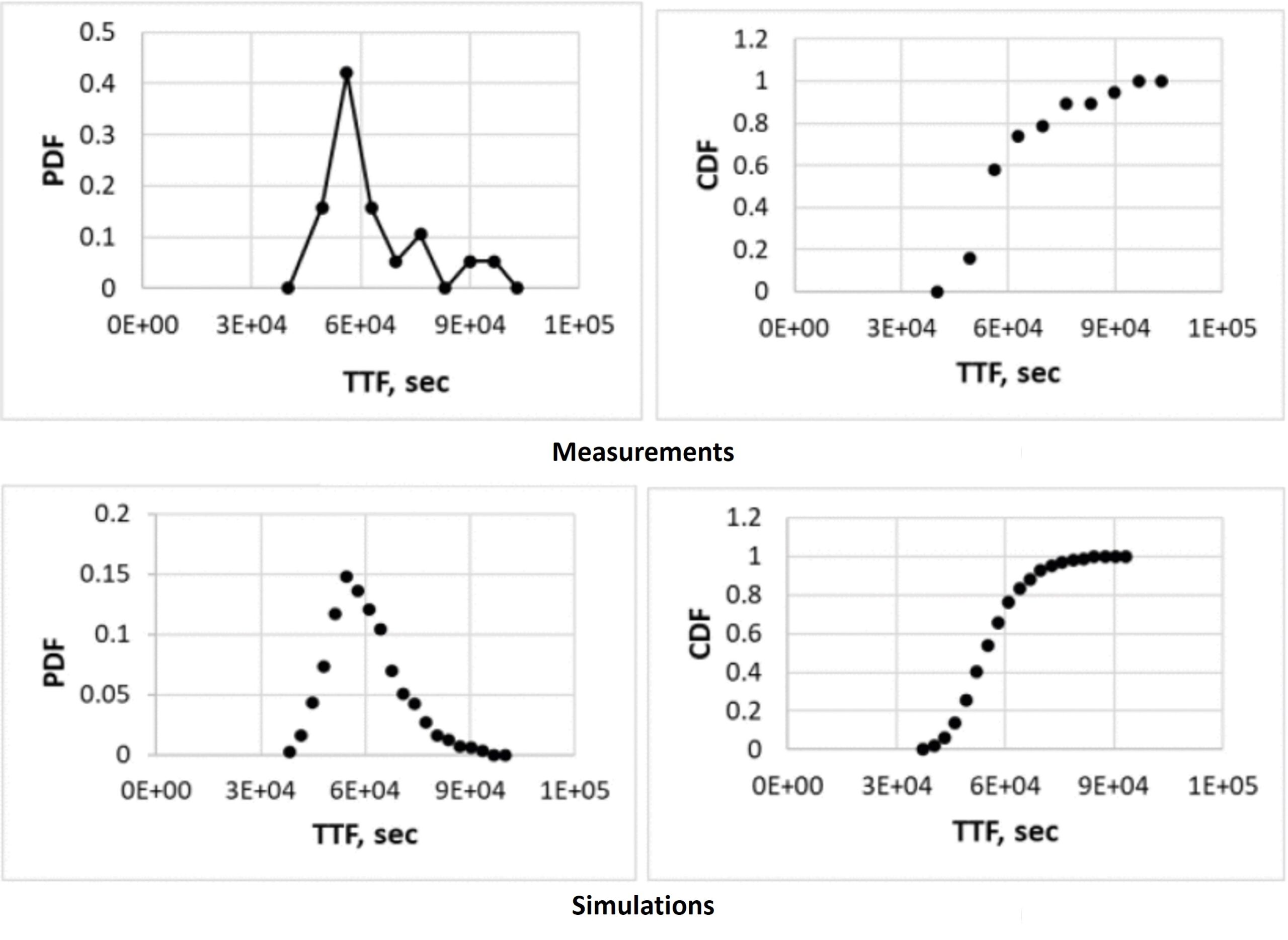
Achieving an accurate assessment of electromigration (EM)-induced failure is essential to developing a realistic estimation of the lifetime of semiconductor chips. Together with colleagues from the University of Toronto in Canada and the University of Minnesota in the United States, we proposed a theoretical methodology for evaluating the EM-induced voltage (IR)-drop degradation in on-chip power/ground grids, and validated our approach with measurements performed on real silicon.
We first employed a voltage tapping technique for direct measurement of voltage variations at 162 nodes of the power net, stressed with 10 mA constant source current at an elevated temperature of 350oC. Any IR drop between cathode and anode pads exceeding a specified threshold was considered a failure. Times-to-failure (TTF) were measured on nineteen packaged test-grids and used for computing the mean-time-to-failure (MTTF). We also analyzed the EM-induced voltage degradation in this grid with an assessment methodology based on a simulation of stress evolution everywhere in the grid, resulting in a voiding in some of grid branches and a corresponding resistance increase. We developed a set of voiding compact models for different grid segments, such as upstream and downstream vias, as well as intra-line voiding, and used them in the simulations. We captured the stochastic nature of the EM phenomenon by introducing random distributions of atomic diffusivities and critical stresses across the grid and iterating them with Monte Carlo loops.
Our results demonstrated a good fit between the measured voltage evolution kinetics at different grid nodes and those predicted by simulation. This good agreement between measured and simulated failure distributions can be considered as the first-ever experimental validation of this EM assessment methodology for on-chip power/ground grids. This physics-based EM assessment approach provides the MTTF for any given power grid, which can be a DC, RC, or RLC netlist, and user-specified current sources and voltages Our approach can reduce the total amount of metal introduced by the iterative widening of metal lines that are close to a void nucleation or voltage drop violation, which is a common industry practice. This trial-and-error technique can iterate forever as it “blindly” tries to fix the grid, and can lead to over-design of the grid. Our developed approach can effectively relax very conservative current density design rules, which can enable improvements in power, time-to-market, and design cost.
In addition to its practical importance, it is also a complex and interesting scientific problem that combines a wide range of topics, from materials science, solid-state physics, and the theory of electrical circuits to statistics and probability, making it as a truly multidisciplinary subject.
A related presentation of this topic at DAC 2022 was awarded Best Presentation. We will also be presenting a follow-on presentation, A Novel Methodology for Electromigration Assessment in On-chip Power Grids with Non-uniform Temperature Distribution: Simulations vs. Measurements, at the 2023 International Symposium on Physical Design this March.
If you would like the complete details, please download a full copy of our paper, Experimental validation of a novel methodology for electromigration assessment in on-chip power grids.