More Than Moore: Finally Crossing the Chasm?
By Michael White, Mentor Graphics
Will fan-out wafer-level packaging be the impetus that pushes 3D-IC into mainstream acceptance?

Let’s take a quick trip through the land of random comments. Which of these sounds familiar to you?
• “Moore’s Law is dead; if not today, then soon.”
• “No one can afford to move to advanced nodes using traditional 2D scaling. “
• “3D-IC (or More than Moore, if you prefer) is going to be the new scaling approach adopted by the marketplace.”
I, for one, have been hearing these pronouncements since pre-20 nm or so, going on the order of 4+ years now. But what have we really observed? Something quite different than these forecasts.
Moore’s Law
As I discussed in my last editorial, contrary to what we read, Moore’s Law isn’t dead. Jumping to the next node may not be the automatic step it once was, but we’re seeing a very healthy number of companies developing designs at 20 nm and below. Following 2D transistor scaling is the conservative approach. For those types of design where it makes sense, companies will continue down this path as long as it’s technically and economically possible to do so.
More than Moore (3D-IC)
Though 3D-IC had some initial success in niche applications, since then it’s been mired in “The Chasm” of the technology adoption lifecycle (Fig. 1), described by Geoffrey A. Moore in Inside the Tornado.(1) We have yet to see broad mainstream market adoption.
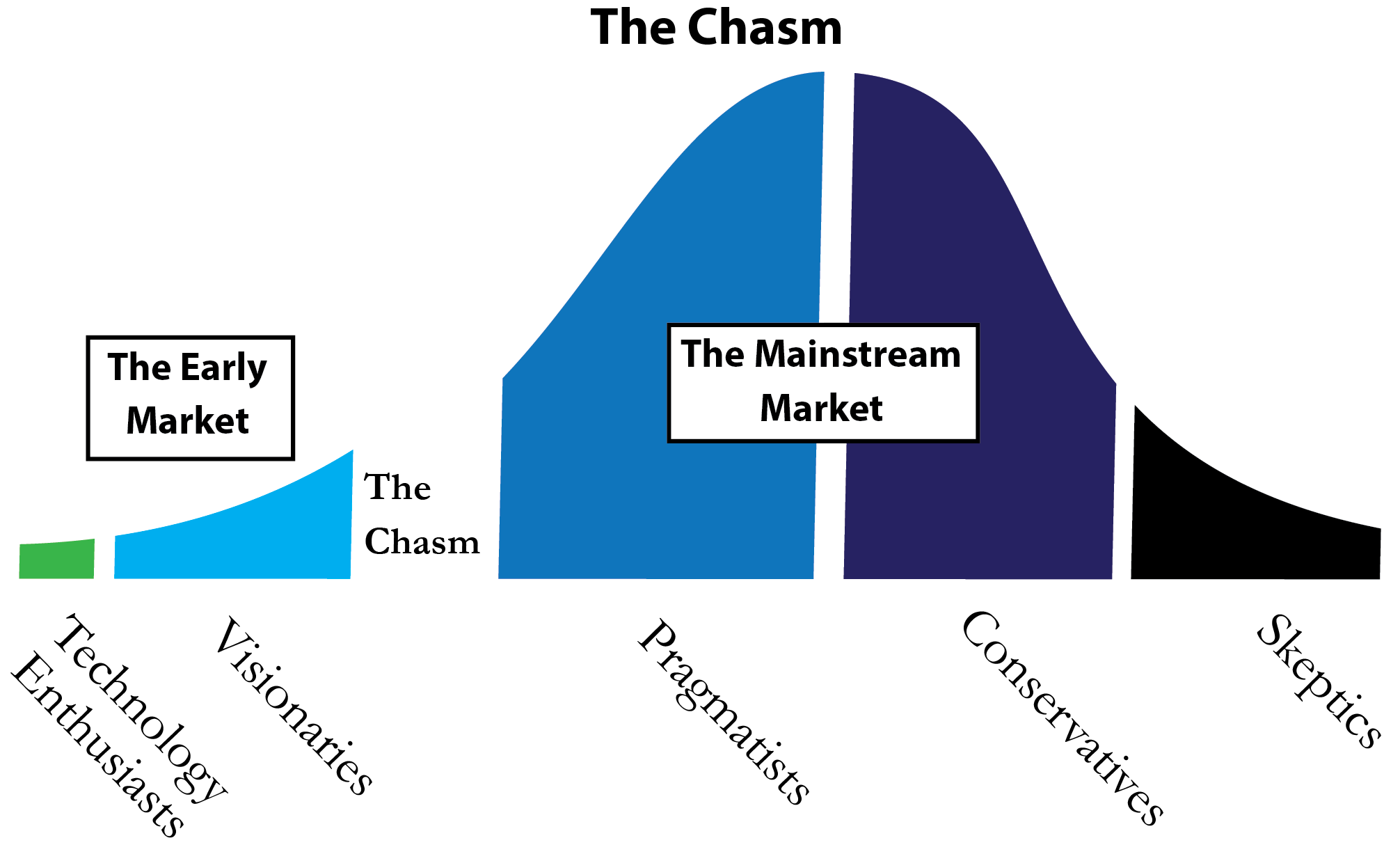
1. The consensus with 3D-IC is that it falls into the Chasm within Moore’s technology adoption lifecycle.
Market-analyst firm Gartner has its own take on this technology adoption lifecycle, with what it refers to as the Gartner Hype Cycle (Fig. 2). In the Gartner model, the “Trough of Disillusionment” lines up with Moore’s Chasm.
3D-IC Successes to Date, and Why
Whether you place it in the Chasm or the Trough of Disillusionment, 3D-IC has had some successes, but has been stalled trying to move into the mainstream market. Let’s take a quick look at some of those successes:
2.5D-IC
• Xilinx implemented a design approach it calls stacked silicon interconnect (SSI), which enables the company to deliver FPGAs with the largest area die and highest bandwidth, with a faster yield ramp, by reducing the size of the individual die to improve the yield of each individual die.(2)
3D-IC
• HiSilicon developed a networking processor solution that combines 16-nm logic chips with a 28-nm I/O chip using TSMC’s heterogeneous CoWoS (Chip-on-Wafer-on-Substrate) 3D-IC packaging process.(3)
• NVIDIA announced the GPUDirect technology that enables GPUs and other devices to directly read and write host and device memory, lowering CPU overhead and reducing latency for computer-intensive workloads.(4)
• AMD’s accelerated processing units (APUs) combine CPU and GPU silicon on a single die in an ongoing effort to create a heterogeneous system architecture and provide cost-effective all-round computing.(5)
What did all of these products have in common? They were all large-die, high-margin products that could afford the incremental cost increase associated with the silicon interposer used to connect the individual die. But what else is out there?
Samsung, Hynix, and Micron created the Hybrid Memory Cube Consortium, whose primary purpose is to build and enable the use of the Hybrid Memory Cube. The Cube is an innovative DRAM memory architecture that combines high-speed logic process technology with a stack of through-silicon-via (TSV) bonded memory die.
Many companies are pursuing the development of silicon-based CMOS image sensors, with a wide range of potential applications—everything from fingerprint pattern imaging to bio-sensing to electronic shutter control. Miniaturizing complex photonic functions on a single chip, with a dense integration of photonics and electronics, enables photonic components with nanometer-scale accuracy over large writing fields, enabling true, large-scale, photonic integrated circuits.(6)
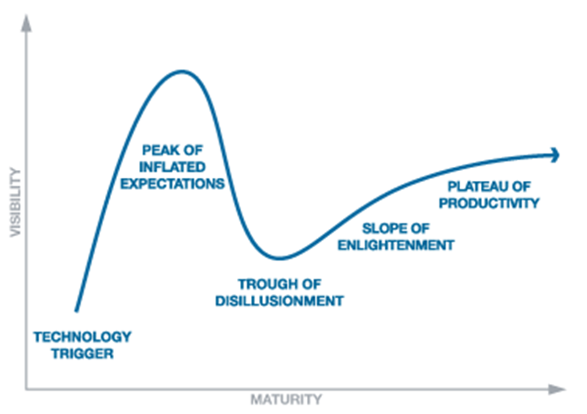
2. Gartner’s technology adoption lifecycle is referred to as the Gartner Hype Cycle.
I think we can draw some interesting observations from these Early Market applications. The original hype surrounding 3D-IC was that it offered a means to continue down a new scaling path by packing transistors closer together, with fine partitioning of logic on adjacent dies. In the Early Market applications we’ve seen to date, this really hasn’t come to pass. These 2.5/3D-IC applications used coarse design partitioning, and gained benefits other than speed by more closely packing transistors. 3D-IC has brought real value to these early applications, but not by solving the Moore’s Law scaling problem, as so broadly predicted.
3D-IC Crossing the Chasm
What has kept 3D-IC from crossing the Chasm or leaving the Trough of Disillusionment up to this point? In my opinion, several things—trying to do too much from the start; being too disruptive to current approaches; lacking both compelling and general customer proofs; and cost. In the technology adoption lifecycle, Early Adopters (i.e., technology enthusiasts and visionaries) want to be first, to embrace new technology and use it as a means to break from traditional approaches and create a compelling competitive/business differentiation.
Conversely, in the mainstream market, Pragmatists are not fans of new technology for its own sake. They prefer making evolutionary changes to their processes, flows, and design methodologies. They want to see compelling success stories from peer companies, as well as solutions from market-leading suppliers, and they want a solution that makes business sense in their conservative world.
TSMC’s 2.5D-IC silicon interposer-based CoWoS reference flow, as well as similar offerings from GLOBALFOUNDRIES and leading outsourced assembly and test (OSAT) houses, were interesting initial efforts to create solutions that the mainstream marketplace could feel comfortable in adopting. These silicon interposer-based advanced packages have had some market success with the Early Adopters. However, from what I hear, they have been limited in a broader deployment due to the cost of the interposer. This cost issue simply boils down to the interposer being another “die” that must be manufactured using traditional wafer lithography processes.
A lower-cost solution could be a game changer, and one looks to be coming with the fan-out wafer-level package (FOWLP), which will be available from an industry-leading source. Per Bernstein Research, TSMC is on track to bring Integrated Fan-Out (InFO) technology, which is TSMC’s variant of FOWLP, to mass production soon.
Bernstein’s Mark Li described some benefits of this new packaging approach, “… InFO removes substrate from package and hence can reduce the thickness of mobile SoC from 1 mm to 0.8 mm or lower.” According to Li, reducing the distance between logic die and the printed circuit board enables quicker thermal dissipation, higher maximal allowable power consumption, and possibly 20% better performance (although with a power penalty).
Conclusions
If this technology achieves market success, as Bernstein predicts, this could be the event that catapults 3D-IC across the Chasm into the Mainstream Market. Such an introduction would check off all the concerns of the typical “pragmatist” by providing a compelling success story from an industry-leading company and a complete solution from a market-leading supplier. To mix metaphors (or models, as the case may be), 2016 should be a really stimulating year for 3D-IC if it finally moves to the Slope of Enlightenment and hits Main Street.
References
1. Moore, Geoffrey A., Inside the Volcano (New York: HarperBusiness, 1995), 14-20.
2. Saban, K. “Xilinx Stacked Silicon Interconnect Technology Delivers Breakthrough FPGA Capacity, Bandwidth, and Power Efficiency.” Xilinx, 2012.
3. Shilov, A. “TSMC builds world’s first 32-core networking chip using 16nm FinFET process technology.” Kitguru, Sept. 25, 2014.
4. NVIDIA GPUDirect Technology, NVIDIA Corp., 2012.
5. Hruska, J. “AMD’s next-gen APU unifies CPU/GPU memory, should appear in Kaveri, Xbox720, PS4.” ExtremeTech, April 30, 2013.
6. Bulayev, Y. “Advances in CMOS Image Sensors Open Doors to Many Applications.” Photonics Spectra.

Liked this article? Then try this –
Article: Reported Death of Moore’s Law Premature?
This article was originally published on www.electronicdesign.com

Comments
Leave a Reply
You must be logged in to post a comment.
Don’t ignore the devices that need to be served,not only today but in the next few years.
The foundries now, on the most advanced nodes, sell perf per dollar, not more since that’s good enough for high end phones. Maybe tomorrow they’ll sell perf per volume.
Phone makers failed to push for reducing PCB volume for thinner devices ,bigger batteries since it was cheaper to reduce volume elsewhere or go with big upper and lower bezels.
With foldable screens it becomes more difficult to find the needed volume- fun fact, volume wise the iphone can pretty much fit the entire battery in the upper and lower bezels.
Watches need low cost and very compact solutions to enable 50-100$ retail prices.
And then glasses, ideally you need very very low power and you simply lack the 2D area needed for the min perf so somehow ,chances are, someone will need to stack logic. Take the thinnest glasses frame and somehow put everything inside it, including the battery, while keeping thermals acceptable.
So, if it becomes more about perf per volume and thermals are a huge problem, can 2D address it anytime soon?
This is an interesting perspective on the topic. Some people view FOWLP as a technology competing with 3DIC. I certainly think that the increased interest in FOWLP in the past 2 years is due to expectations unmet by 3DIC (and interposer-based technologies). The takeaway from your article seems to be that FOWLP may help advance 3DIC rather than compete with it. I don’t fully grasp the reasoning behind this, however. If more FOWLP technologies are coming onto the market, in what way will they promote the use of interposer-based and 3D technologies?