Extraction Challenges Grow in Advanced Nanometer IC Design
By Carey Robertson, Mentor Graphics
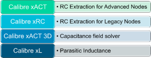
The Calibre xACT platform is a new type of extraction tool that provides a range of extraction techniques to accurately process new parasitic extraction challenges at advanced nodes, while still enabling fast runtimes and scalability.

Successive generations of foundry process technologies enable ever-increasing design density, performance, and power savings, if only designers can deal with growing challenges.
Innovative new process features such as FinFET transistors require a significant increase in the accuracy of parasitic extraction — the creation of an accurate analog — for simulation and analysis to verify performance of the physical design. Here are some of the new extraction challenges and how tool technology has evolved to meet the new requirements.
What drives new tool requirements
Integrated circuit designers need to extract the detailed electrical properties of an IC after it has been committed to a specific physical layout so they can do static analysis and simulation to ensure the IC will function properly and meet critical performance requirements. Especially at 16nm and below, it is paramount to accurately capture the parasitic resistance and capacitance within FinFET devices, as well as the interactions between devices and the parasitics associated with interconnect wires. In addition, there are variations in the way different foundries model their FinFET devices. For example, some foundries use floating devices between the designed FinFETs, so it is important to capture coupling to the floating devices and between the main active devices. Parasitic resistance within the FinFET is also important—as the fin channel and the source-drain regions narrow, increased source-drain resistance degrades device performance.
Double pattering exacerbates the problem because any misalignment of masks during manufacturing impacts the predictability of parasitic capacitance by increasing or decreasing the distance between features on multi-patterning layers. Consequently, designers need to characterize potential misalignment by performing simulations with multi-patterning corners. In practice this often means a combination of more than 10 process, temperature and double patterning (DP) corners. The time spent on a big, full-chip design to extract all the necessary corners could easily exceed the typical 8-10 hour (overnight) full-chip run with traditional tools. Designers are sometimes forced to limit their timing analysis runs to a few well-chosen corners for the sake of expediency, increasing the risk of missing a critical corner combination.
Another challenge is the escalating amount of fill data associated with large, advanced node designs, which presents a considerable burden to parasitic extraction tools. They must read and process gigabytes of data in order to accurately model the density and parasitic capacitances of wires adjacent to fill patterns. Processing this data quickly and producing a compact fill model is essential to maintaining throughput and managing memory usage of extraction tools.
More accuracy, more complex models, and more corners multiply the already awesome challenge of handling a node-to-node exponential increase in device count and interconnect complexity, making for a huge extraction computational task at advanced nodes. Yet design teams want the same turnaround time they’ve enjoyed at older nodes—specifically, they want to be able to do full-chip extraction overnight so they can continue design work the next day.
New tool approaches
Meeting these new challenges has forced EDA vendors to go back to the drawing board and create completely new extraction architectures. In the case of Mentor, we wanted to deliver a tool that could:
- Provide accuracy rivaling reference extraction tools (which tend to be quite slow)
- Deliver turnaround time consistent with rule-based tools (which tend to be less accurate)
- Extract detailed FinFET device models
- Support simultaneous multi-corner extraction
- Incorporate multi-patterning natively in the extraction flow
- Employ extremely fast and efficient extraction algorithms
- Provide a consistent solution that spans full-chip signoff and IP characterization
- Enable fast downstream simulation with advanced reduction techniques
- Support massively parallel processing methods
- Be highly scalable across many CPUs in both SMP and networked configurations
To meet all these requirements takes several innovations working together to deliver the sought-after capabilities. Firstly, to get the best accuracy requires a field solver, which does what the name implies—it solves Maxwell’s differential field equations in three dimensions. At Mentor we use some innovative computational methods, which are both efficient and highly parallelized, to enable the field solver engine to run orders of magnitude faster than traditional reference field solvers. This provides the needed accuracy — in the attofarad range — without a severe performance penalty. This is a deterministic technique (versus Monte Carlo probabilistic approaches) that delivers repeatable results with mean error close to zero and low standard deviation.
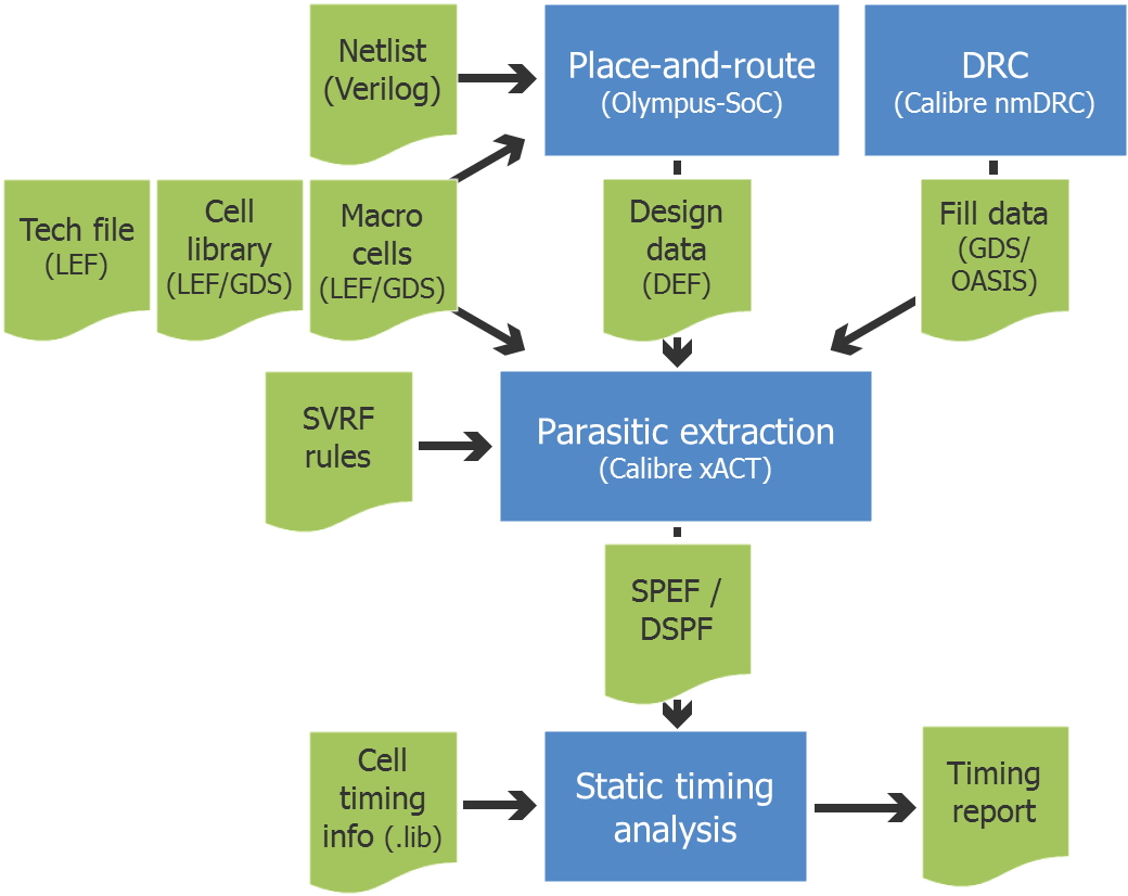
The new Calibre xACT extraction tool fits in the digital flow between the place and route and static timing analysis (STA) steps, providing information about parasitic and coupling effects that is essential to STA tools.
Net-based parallelism and multi-CPU processing
To achieve nearly ideal linear scaling with massively parallel processing, we introduced a new approach to decomposition. Rather than the typical tiling method, which breaks up nets into many pieces that are processed separately, we keep each net intact and process each entire net on a dedicated CPU. This net-based parallelism approach eliminates boundary and halo effects on accuracy, and provides better scalability than tiling, especially on symmetric multiprocessing (SMP) machines. Net-based parallelism also eliminates variance in the accuracy of results that occurs with tiling when the number CPUs changes.
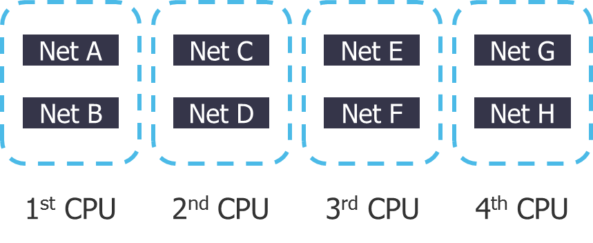
With net-based parallelism, each net is sent to a single CPU. Since each net is processed intact, and not tiled, this method provides a highly accurate solution with excellent scalability.
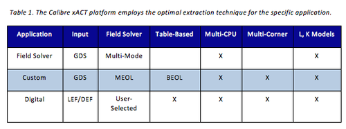
To further improve performance, the new architecture employs highly scalable rule-based techniques where less accuracy is needed, such as in the upper metal layers. Table 1 shows how the appropriate extraction technique is automatically selected for different geometries and layers.
The result of these innovations working together is a 3X extraction performance improvement, or about 4-8 million nets per hour with 8 CPUs, and accuracy that meets leading edge foundry signoff requirements. With the new Calibre xACT architecture, it takes about 15 minutes to extract a 1 million net block, and full chip extraction on a design with 20 million nets completes overnight. Larger designs can be handled by adding additional CPUs.
For designs that require many extraction corners, the new platform performs simultaneous multi-corner extraction with about a 15-20% runtime increase for each additional corner, and no loss in accuracy. Because it uses a deterministic technique, single corner and multi-corner runs deliver the same results, which is not always the case for Monte Carlo approaches.
Selective net processing and netlist reduction
Another way to speed up turnaround time and also reduce the volume of data to manage is a technique called selective net processing. This enables designers to tailor the amount of data generated for simulation by selecting the specific parasitic model they want for each net. Designers can select distributed RCC (with coupling capacitance), RC (no coupling capacitance), C, or R on a net-by-net basis. They can also control extraction by layer. For example, to reduce simulation time while taking into account the parasitic effects for large power and ground nets, designers can extract VDD and VSS nets including only via resistance, and excluding metal layer resistance. This is useful because vias contribute the most resistance to the power/ground net. This enables faster simulation while still maintaining the required design margins.

Calibre xACT has selective processing capabilities. In this example, a netlist is generated with different net models for different types of nets. For power (VDD) and ground (VSS) nets, only via resistance is extracted into the netlist. The critical differential pair nets PLUS and MINUS are extracted in RCC mode, and all of the other nets will only contain total capacitance values.
Another time-saving approach is to generate multiple netlists from a single parasitic extraction database (or extraction run). This can be used to generate multiple netlist formats as well as netlists with multiple parasitic models, which can be controlled on a per-net basis. This saves time because extraction doesn’t have to be run every time a different netlist needs to be generated, and enables multiple post-layout analyses from a single extraction run. For example, a designer can perform a single RCC extraction run on all nets in the design, and then generate a SPICE netlist with RCC net models for all signal nets to do a timing analysis, followed by a resistance-only netlist in DSPF format for electromigration analysis.
Simulator performance is highly dependent on the size of the netlist, and parasitic elements can increase netlist size by orders of magnitude. More accuracy means more parasitics, but the circuit becomes more difficult and lengthy to analyze. That’s why flexible netlist reduction techniques are important to minimize the amount of parasitic data generated for post-layout simulation to just what is needed (see chart below). This speeds up simulation performance and reduces analysis time and convergence problems.
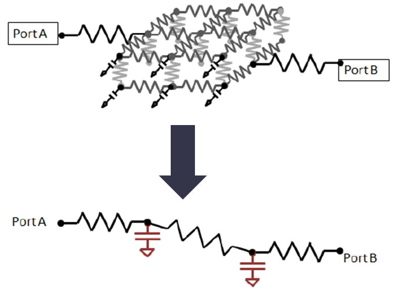
Designers can fine tune netlist reduction settings to control the level of accuracy and netlist size as needed. In this example, the via array is reduced to a much smaller size, enabling faster simulation while retaining accuracy.
EDA vendors stepping up
Digital, custom, analog or RF design teams working at any node, but particularly at 16 nm and below, require an extraction tool that is faster, more accurate, and more flexible than previous generations of can provide. EDA vendors are stepping up to the challenge with new extraction tools built on more advanced architectures and algorithms to deliver the needed capabilities.
Author
Carey Robertson is a director of product marketing at Mentor Graphics Corp., overseeing the marketing activities for Calibre PERC, LVS, and extraction products.

Liked this article? Then try this-
Video: The Calibre xACT Platform: Next-generation parasitic extraction for 16 nm and beyond
This article was originally published on www.eetimes.com

Comments
Leave a Reply
You must be logged in to post a comment.
Hi. Thanks for this article. Do you have any thoughts you can share on any unique challenges SADP presents to parasitic extraction? Thanks!