Designing and Testing FinFet-based IC Designs
By Carey Robertson and Steve Pateras, Mentor Graphics
Are your processes ready for finFETs?

The emergence of FinFET transistors has had a significant impact on the IC physical design and design-for-test flows. The introduction of FinFETs means that CMOS transistors must be modeled as three-dimensional (3D) devices during the IC design process, with all the complexity and uncertainty this entails. The BSIM Group of the UC Berkeley Device Group has developed a model, known as BSIM-CMG (common multi-gate), to represent the resistances and capacitances that exist within FinFETs. The foundries have also worked very hard to provide accurate device and parasitic data, as well as to preserve the use-model employed for previous processes.
Extraction Challenges
However, each foundry modifies the standard model to more closely represent its specific architecture and process. Additionally, at these advanced process nodes, the foundries desire a much tighter correlation between the ‘gold’ models they have built using reference field solvers, and the output of extraction tools that designers use in the field. At the 28 nm node, foundries want commercial extraction tools to be within 5% to 10% of their gold models. For FinFET processes, foundries require a mean accuracy error within 2% of the gold model, and a three-sigma standard deviation of just 6% to 7%.
The most challenging task is accounting for the more complex, unintended interactions between FinFETs and their surroundings, which requires accurate 3D modeling for Front End of Line (FEOL) geometries. Getting accuracy in three dimensions requires the use of 3D field solvers for extraction. These were previously used for process characterization, not design, because they were too expensive computationally and too slow. Now there is a new generation of 3D extraction tools, such as Mentor’s Calibre® xACT, that run an order of magnitude faster by employing adaptive gridding techniques to speed up computation. They also have a highly-scalable architecture to take advantage of multiple CPU’s in modern compute environments. With these features, an extraction tool can comfortably perform a field solver computation solution on designs ranging from small cells to large blocks incorporating several million transistors on a 32 CPU machine.
At the full-chip level, we need to consider multi-billion transistor designs with tens of millions of nets where even fast field-solvers cannot provide a practical turnaround time. The solution is to employ advanced heuristics to leverage the field solver for complex structures, then switch to table-based methods for more regular geometries. This is feasible because modeling the electrical field in the wiring grid is similar to what was seen at previous nodes. In the best case, the extraction use model for designers won’t change because the tools will automatically move between field-solver and table-based methods.
With double and triple-patterning playing an increasing role in manufacturing starting with the 20 nm node, we are also experiencing a big jump in the number of interconnect corners. At 28 nm, five interconnect corners are likely, but at 16 nm, we expect to need 11-15 corners. Advanced multi-corner analysis schemes can enable more efficient computation, reducing the amount of additional computing required for each additional corner. In addition, we can process corners in parallel, so that each additional corner adds only 10% to overall turnaround time. This means that 15 corners now only require 2.5X the run time of a single corner.
Test Challenges
Test and failure analysis are of particular importance because FinFET critical dimensions are for the first time significantly smaller than the underlying node size. This has led to growing concern over increased defectivity levels as well as increased yield challenges. The Cell-Aware test methodology is particularly well suited to addressing these issues because it can target defects at the transistor level. This is in contrast to traditional scan test patterns, which can only find defects in the interconnects between cells. The Cell-Aware analysis process creates a set of fault models based on the simulated behavior of defects within the cell layout. As a result, a higher quality pattern set can be produced. Silicon results across a large range of technology nodes, from 350nm to FinFETs, have shown significant additional defect detection beyond standard stuck-at and transition patterns when using Cell-Aware ATPG.
Consider a multi-fin FinFET transistor with three fins. Recent research suggests that two defects types should be considered for such transistors: leakage defects that force the transistor partially or completely on, and drive-strength defects that force the transistor partially or completely off.
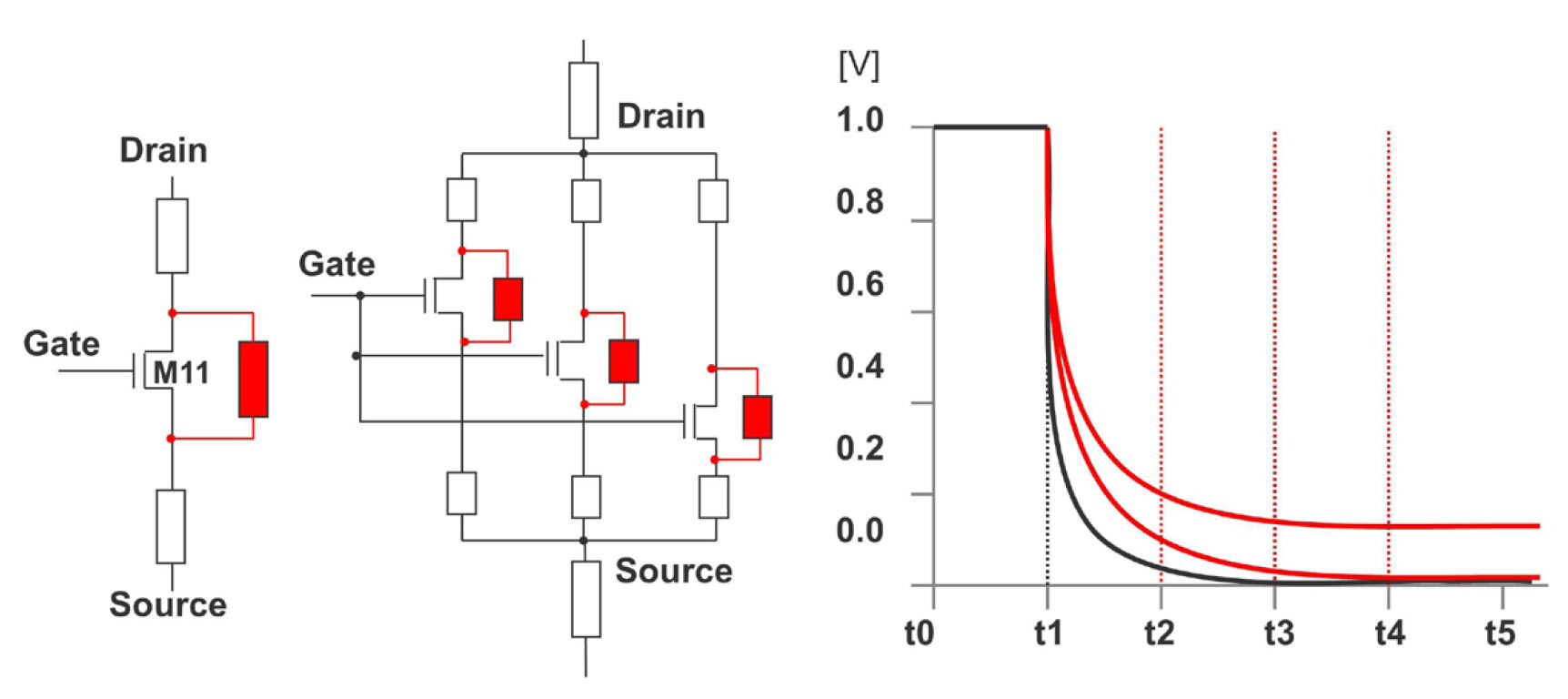
Figure 1. Testing for FinFET leakage defects.
The leakage defects can be analyzed by placing a resistor across the gates (from drain to source) of each of the transistor’s three fins as shown in Figure 1. During the Cell-Aware analysis process, analog simulation is performed with varying resistive values for all resistors for all FinFETs in a given library cell. Defects are modeled for cases where the transistor’s response is delayed by a certain threshold. Drive-strength defects can be analyzed by placing a resistor between the drain and each of the fin’s gates and between the source and the fin’s gates. As with the leakage test, analog simulation is performed with varying resistive values for each of the resistors. Differences in the response time of each fin are used to determine when a defect is to be modeled. Additional FinFETs defect types can be handled in a similar fashion.
FinFETs do create some new challenges, but EDA tool vendors and foundries are doing their best to incorporate solutions in a way that has minimal impact on the IC design flow.
Authors
Carey Robertson and Steve Pateras are product marketing directors at Mentor Graphics.
The article was originally published on www.semiengineering.com