Part 4: The 2018 Wilson Research Group Functional Verification Study
This blog is a continuation of a series of blogs related to the 2018 Wilson Research Group Functional Verification Study (click here). In my previous blog (click here) I discussed verification effort trends in terms of project time spent in verification, as well as increasing headcount as indicated by the rising mean peak number of design and verification engineers working on FPGA projects. In this blog I continue the discussion of FPGA verification effort trends by looking at where engineers spend their time.
FPGA Verification Effort Trends Continued
Where FPGA Design Engineers Spend Their Time
Verification engineers are not the only project stakeholders involved in the verification process. Design engineers spend a significant amount of their time in verification too, as shown in Fig. 4-1. In 2018, design engineers spent on average 56% of their time involved in design activities and 44% of their time in verification. However, the data indicates a trend that FPGA design engineers are spending less time involved in verification tasks. There are two reasons for this trend. First, many FPGA projects have added verification engineers to their teams, which means design engineers can focus most of their effort on design. Second, in general, there has been increased adoption of larger, more complex FPGAs, which has increased the design engineer’s workload.
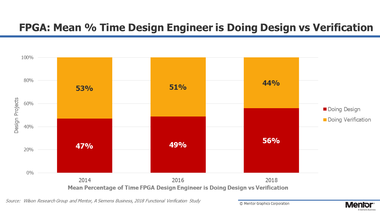
Figure 4-1. Where FPGA design engineers spend their time
Where FPGA Verification Engineers Spend Their Time
Fig. 4-2 shows where verification engineers spend their time (on average). We do not show trends here since there were no significant changes in the FPGA results during the period 2014 through 2018.
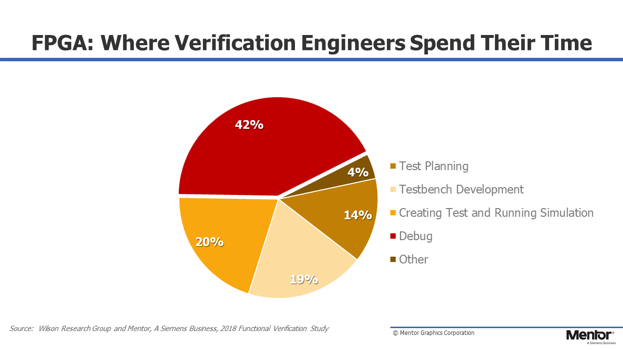
Figure 4-2. Where FPGA verification engineers spend their time
Our study found that FPGA verification engineers spend more of their time debugging than with any other activity. From a management perspective, this can be a significant challenge when planning future projects’ effort and schedule based on previous projects’ data since debugging is unpredictable and varies significantly between projects.
The key takeaway here is that a significant amount of engineering time is spent in the verification process when you consider the combined design and verification engineering time.
In my next blog (click here) I shift the focus of our discussion from verification effectiveness and effort trends to FPGA verification technology adoption trends.
Quick links to the 2018 Wilson Research Group Study results
- Prologue: The 2018 Wilson Research Group Functional Verification Study
- Understanding and Minimizing Study Bias (2018 Study)
- Part 1 – FPGA Design Trends
- Part 2 – FPGA Verification Effectiveness Trends
- Part 3 – FPGA Verification Effort Trends
- Part 4 – FPGA Verification Effort Trends (Continued)
- Part 5 – FPGA Verification Technology Adoption Trends
- Part 6 – FPGA Verification Language and Library Adoption Trends
- Part 7 – IC/ASIC Design Trends
- Part 8 – IC/ASIC Resource Trends
- Part 9 – IC/ASIC Verification Technology Adoption Trends
- Part 10 – IC/ASIC Language and Library Adoption Trends
- Part 11 – IC/ASIC Power Management Trends
- Part 12 – IC/ASIC Verification Results Trends
- Conclusion: The 2018 Wilson Research Group Functional


Comments