Automotive Semiconductor Test
By Steve Pateras, Mentor Graphics
Ensure quality and reliability in automotive ICs with the newest technologies in silicon test.

We are witnessing the gradual transition of the automobile from a simple means of transportation to a mobile electronic hub. The amount of electronic content in passenger cars continues to grow rapidly. Recent reports indicate that electronics now contribute about 40% of the total costs of a traditional, internal combustion engine car, and this jumps as high as 75% for the growing number of electric and hybrid-electric vehicles. The amount of electronics will only continue to grow as manufacturers continue to add new advanced safety features, greater information and entertainment services and improvements in energy efficiency. Safety features are experiencing particularly large growth and encompass items such as collision avoidance, lane change assistance and automatic parking. The industry’s move towards fully autonomous vehicles promises to even further increase the number of these safety features.
The electronic components behind these safety features, as well as any other electronics involved in the operation of the vehicle, need to meet extremely high quality and reliability metrics. To ensure consistency across the large and growing number of automotive suppliers, an international automotive components safety standard was established. Called ISO 26262, the standard defines the requirements for building safe automotive equipment and is being rapidly adopted by automotive manufacturers and suppliers worldwide. The standard is comprehensive and covers all aspects of the hardware and software lifecycle from design through testing and in-field operation.
The Mentor Tessent product family offers several solutions for helping to address the quality and reliability metrics mandated by the standard. Solutions exist for increasing both the manufacturing test quality as well as the long term reliability of automotive parts.
ACHIEVING VERY LOW DPM WITH CELL-AWARE TEST
The widely used methodology for testing digital circuits is to add scan test structures to the design and then deliver test patterns through these structures that reveal defects when the chip responses are observed. The approach has been in use for decades and is based on modeling circuit defects to a level of abstraction that enables a computationally efficient test pattern generation process. The simple stuck-at fault model, which models circuit defects as logic nets stuck at either a 0 or 1 value, was initially used. More complex fault models were added over the years to account for new defect types that appeared as the industry transitioned to new technology nodes. Among the more recently adopted fault models were the transition, bridging, open and small-delay faults.
However, with the move to smaller geometries these fault models and associated test patterns are becoming less and less effective at ensuring desired quality levels. The main problem is that all of these existing fault models only consider faults on cell inputs and outputs and on interconnect lines between these cells. In other words, only faults abstracted to the netlist level are explicitly considered.
It turns out, however, that increasingly more defects occur within the cell structures. For the more advanced technology nodes and associated fabrication technologies between 130 nm and 90 nm, the number of defects found within cells to represent half of all circuit defects and has been increasing in each successive technology node. Thousands of patterns are typically produced during the normal ATPG process. As a result, although traditional fault models do not target cell-internal defects, many of these defects end up being detected by chance. However, when considering millions of gates in a design, it is not effective to rely on luck to detect potential defects within each cell.
One option would be to apply every possible combination of inputs at every gate. This fault model is referred to as the gate-exhaustive fault model. It would certainly be effective in detecting all static cell-internal defects since it would apply every possible combination. For example, for an 8 input cell, gate-exhaustive testing would apply all possible 28 = 256 input combinations. It is easy to see that applying such an exhaustive set of patterns quickly becomes impractical. To make matters worse, many defects inside cells are timing related and therefore are not detectable using static tests. A two-pattern test is necessary to detect such defects. So for the 8 input cell example, two-cycle gate exhaustive testing would require the application of 28 x 28 = 65,536 patterns. For designs with very high quality requirements such as those looking to comply with the ISO 26262 standard, a much more efficient test strategy for detecting cell-internal defects is clearly necessary.
A recently introduced ATPG-based test methodology achieves the needed efficiency improvements by directly targeting specific defects internal to each cell [1]. The cell-aware test approach starts with an automated cell library characterization process, which is illustrated in Figure 1.
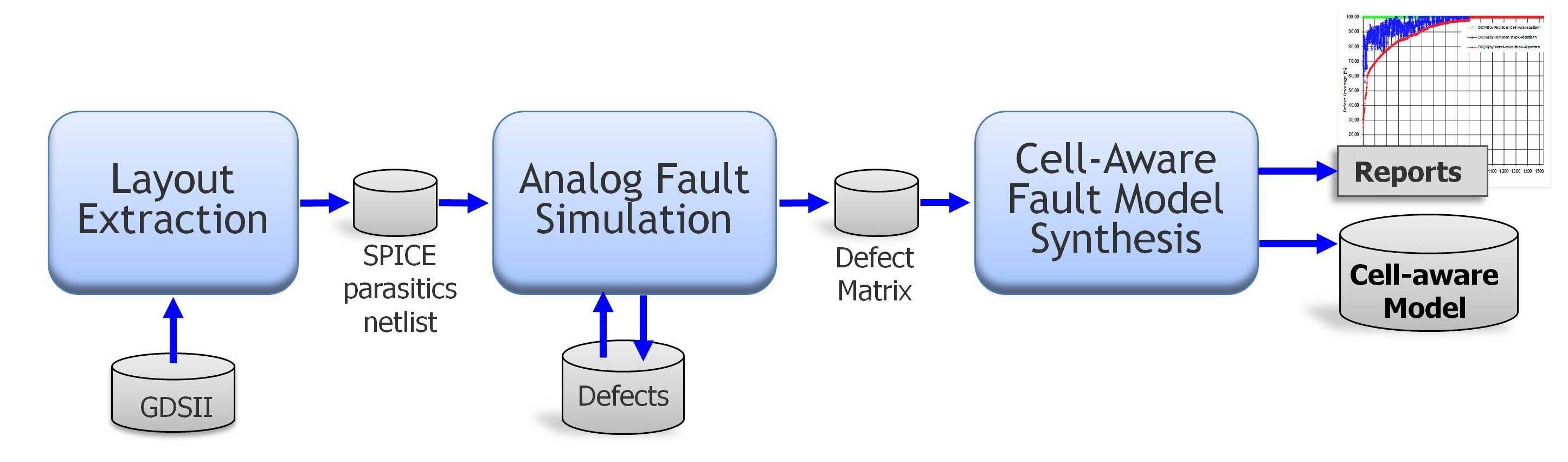
Figure 1: Generating cell-aware fault models through library characterization.
Each semiconductor process node has a set of technology cell libraries used to describe the logic behavior and physical layout of the lowest level component in the netlist. The cell-aware characterization process starts with an extraction of the physical library, represented in GDSII. Each extracted cell results in a transistor-level netlist with parasitic resistances and capacitances. A resistance location represents a conductive path with the potential for an open defect, while a capacitance identifies locations with the potential for a bridge defect. An analog simulator is then used to simulate each potential defect against an exhaustive set of stimuli to determine if there are sets of cell inputs that produce an output different than the defect-free result. The simplest case is to simulate each capacitive location with a 1-ohm resistance representing a hard bridge. Many other resistive values can be used as well with some resulting in different test stimuli requirements. In addition, simulating over multiple cycles is also useful to detect bridges or opens that are only observed as dynamic defects.
The final process in cell-aware characterization is to convert the list of input combinations into a set of the necessary input values for each fault within each cell. Because this information is defined at the cell inputs as logic values, it is basically a logic fault model representation of the analog defect simulation. This set of stimulus for each cell represents the cell-aware fault model file for ATPG. Within this file, a simulated defect (now a fault) can have one or more input combinations. Note that because the cell characterization process is performed for all cells within a technology library, any design using that technology can read in the same cellaware fault model file. Characterization only needs to occur once and then can be applied to any design on that technology node.
Silicon results have shown significant additional defect detection beyond standard stuck-at and transition patterns when using cell-aware ATPG. These detection improvements have been measured at various technology nodes from 350 nm down to 32 nm and below. Perhaps more importantly, these improvements have been achieved with modest increases in test application times. The defect coverage improvements obtained using cell-aware test patterns can also result in other test benefits. With these improved results, it may become possible to reduce or eliminate other costly test procedures such as performance margining or system-level testing.

Figure 2: DPM improvements with cell-aware ATPG.
ENSURING SYSTEM RELIABILITY WITH IN-LINE SELF-TEST
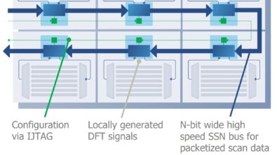
Improvements to test quality and efficiency for ISO 26262-compliant ICs standard can be achieved using a new hybrid test solution, which combines both ATPG compression and logic BIST techniques. Although these solutions have historically been used independently and typically for different applications, they possess complimentary features that turn out to be very beneficial in combination. The two solutions also make use of much the same on-chip DFT resources. For example, they both make use of scan chains and related test clocks. The main difference between the two solutions lies in the on-chip logic feeding test data to the scan chains and processing the test response data coming out of the scan chains. It turns out, however, that there are also similarities in this logic so the logic of the two solutions can be effectively combined to support both approaches. A diagram illustrating the high-level architecture for the hybrid solution is shown in Figure 3.
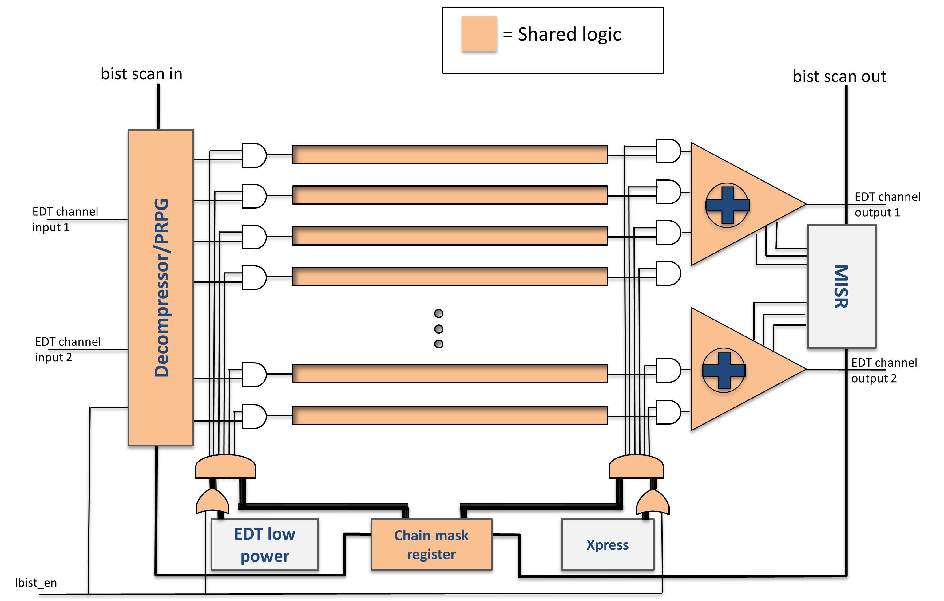
Figure 3: Hybrid ATPG Compression and Logic BIST Architecture.
Most of the on-chip resources shown in the diagram are common to both test approaches. The only resources unique to one approach or the other are the EDT low-power and Xpress modules used for ATPG compression and the multiple-input signature register (MISR) module used by the logic BIST solution. In addition to efficient sharing of resources, both ATPG compression and logic BIST capabilities can also be integrated into the design using common flow automation capabilities, adding to the overall efficiency and value of the solution.
Another critical area addressed by the ISO 26262 standard is long-term device reliability. A number of techniques are already in use by many semiconductor manufacturers towards achieving the necessary reliability levels, including methods such as functional redundancy, error correction and built-in self-test. The hybrid solution therefore plays another critical role related to the ISO 26262 standard. The solution’s logic BIST capability can be combined with other common BIST capabilities, such as memory BIST, to provide in-system test coverage for most, if not all, of the design. All of the BIST capabilities can generally be accessed through the standard IEEE 1149.1 TAP controller interface.
A dedicated TAP interface is sometimes not accessible in-system. There are multiple options to accommodate in-system access. The TAP controller can be enhanced to also support a generic CPU interface that translates between parallel read/write CPU operations and the serial bit sequences required by the TAP protocol. For situations where a fully autonomous power-on self-test (POST) capability is required, a test controller can instead drive the TAP controller, as illustrated in Figure 4.
When activated by a power-on reset signal, this test controller automatically applies the necessary serialized sequences to the TAP to perform any needed BIST initialization and activation. This controller can be made fully programmable with test sequence instructions stored in an embedded memory. If even more automation is required for a very fast initialization, a pre-set configuration can be present at start-up to immediately begin the logic BIST operation. If necessary, the BIST patterns can be paused and resumed later.
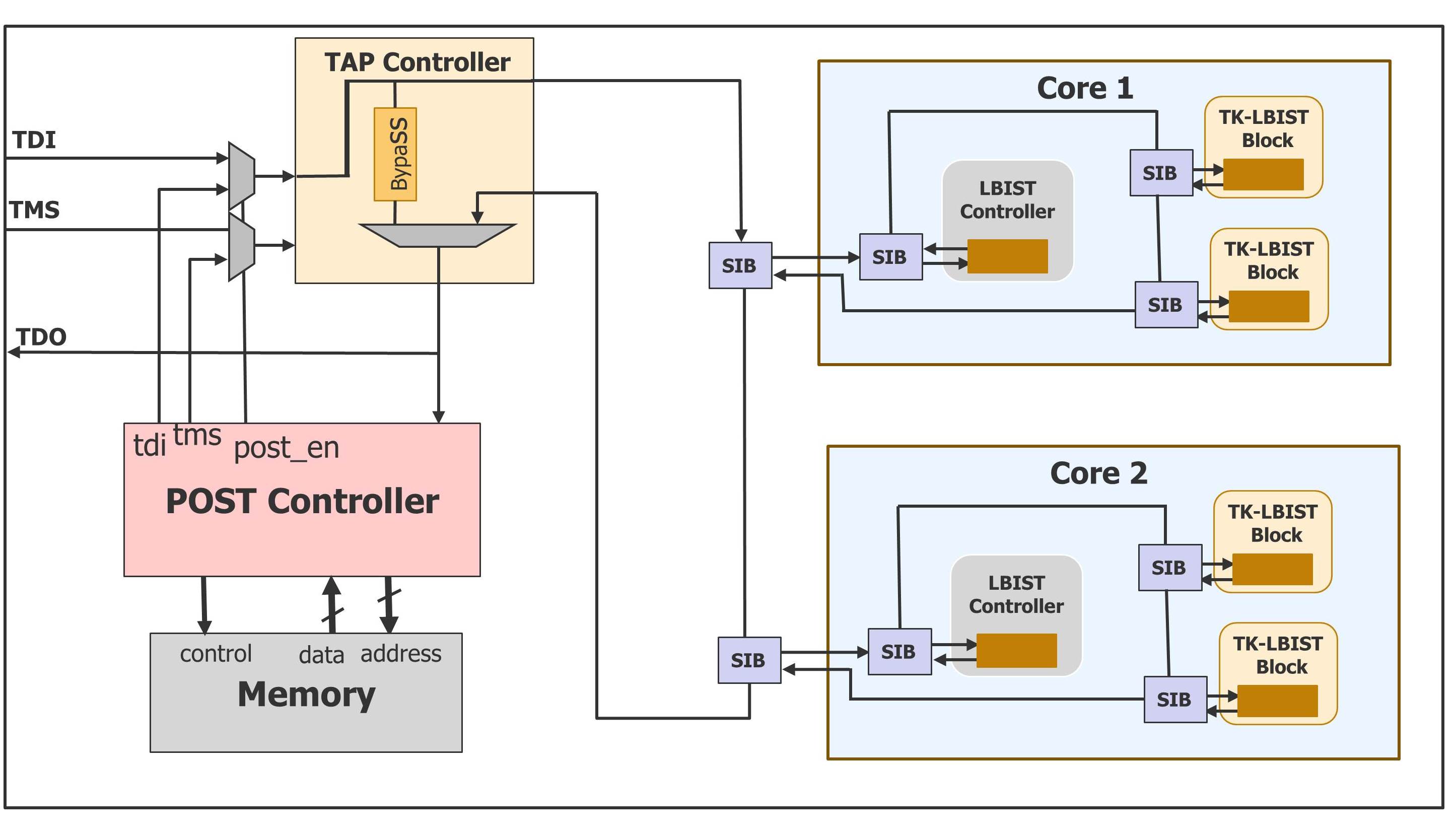
Figure 4: Programmable Power-On Self-Test Architecture.
YIELD EXCURSION ANALYSIS FOR RELIABILITY IMPROVEMENT
Yield excursions can occur even for the more mature processes that are typically used for automotive parts. The underlying cause of an excursion may have an effect on long-term reliability. Quickly identifying and correcting the problem is therefore important.
Mentor’s diagnosis-driven yield analysis (DDYA) technology can rapidly identify the root cause of yield loss and effectively separate design- and process-oriented yield loss components. In a previously published case, Freescale used the results from diagnosis analysis of 1300 failing die to improve mature yield by 1.5% in a few weeks [2]. New advances in diagnosis analysis technology make DDYA more valuable than ever before.
DDYA has two key components. First, as illustrated in Figure 5, scan diagnosis software makes failing test cycles valuable by identifying defect locations and classifications based on the design description, scan test patterns, and tester fail data.
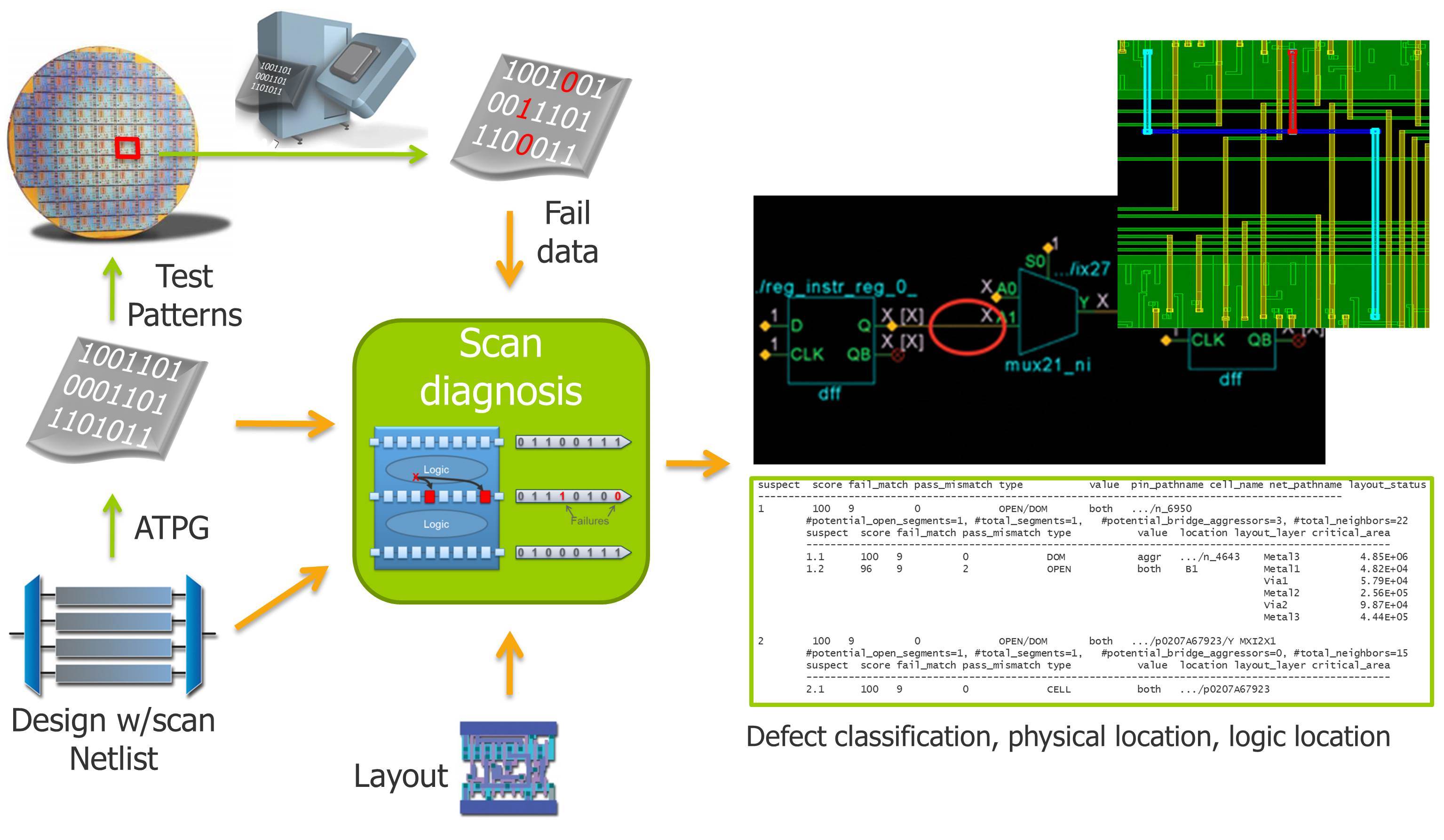
Figure 5: Layout-aware scan diagnosis identifies the location and classification of defects in digital semiconductor devices.
The second component in a DDYA flow is the statistical analysis, which makes the diagnosis results from a number of failing devices actionable. The primary challenge for yield analysis based on diagnosis data is dealing with the ambiguity in the results. For example, the defective behavior seen on the tester could be explained by a defect in more than just one single location. Second, each diagnosis result, often referred to as a suspect, could have multiple possible root causes associated with it. To effectively eliminate the noise in the diagnosis results and determine the underlying root causes represented in a population of failing devices, there is a new technology called root cause deconvolution (RCD) [3]. This technology is based on Bayesian probability analysis, which is well-known in machine learning applications. It leverages design statistics such as critical area per net segment per metal layer and count of tested cells per cell type. The technology uses a probabilistic model that calculates the probability of observing a set of diagnosis results for a given defect distribution. This model is in turn applied to determine the most likely defect distribution for a given set of diagnosis results.
A typical RCD analysis flow is shown in Figure 6. Layout-aware diagnosis is performed on a set of die that failed manufacturing test (1). Each diagnosis result contains a set of root causes that are potential explanations for the failure. If we add up all the root causes and count the number of die whose failure could be explained by each root cause, we get a diagram that includes all the real root causes as well as the noise (2). RCD then eliminates this noise and identifies the underlying root cause distribution (3). From this distribution, the user can focus on the most significant root cause, or on a root cause that has not been seen before or for other reasons is unexpected. Along with the root cause distribution, RCD assigns a probability for root cause per diagnosis suspect (4). This means that the user can easily identify the die that has the highest probability of representing a particular root cause, and use that as way to select die for failure analysis (FA). When comparing the RCD results to the original diagnosis report for one failing die, we see that RCD has eliminated several of the original root causes, thus effectively improved the resolution for that individual result (5). In this particular example, the original report contained 7 possible root causes for one failing die, while RCD limited this to one single result. The layout snapshots show the defect bounding boxes before and after RCD (6).
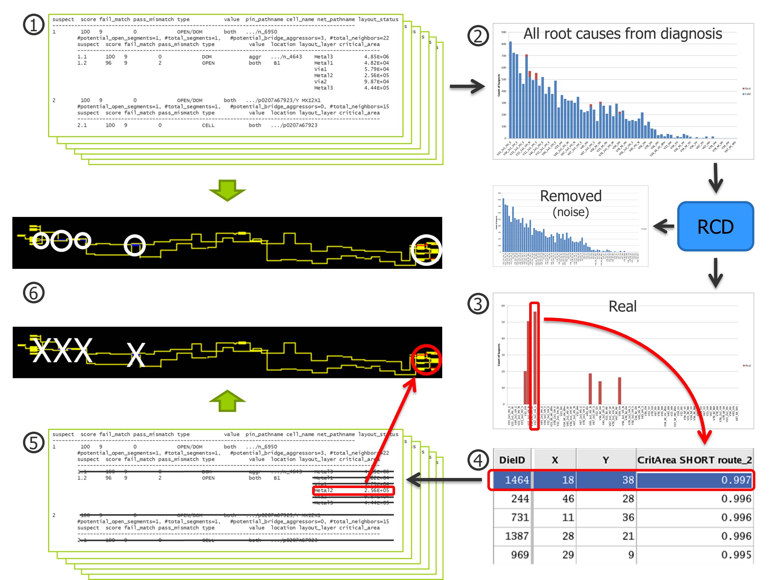
Figure 6: Root Cause Deconvolution determines the root cause distribution and devices most likely to fail for each root cause.
Diagnosis-driven yield analysis with RCD is a quick and cost effective way to determine the underlying root causes represented in a population of failing devices from test data alone. This technology can ferret out the final 1% yield loss in mature technologies typically used for automotive parts.
CONCLUSION
Meeting the quality and reliability requirements of the ISO 26262 and other automotive electronics standards will only become more difficult as device sizes and complexities continue to grow. New advanced test technologies such as cell-aware ATPG, hybrid compression/logicBIST and diagnosis-driven yield analysis with RCD provide some key building blocks towards ensuring compliance to the new standards. Adoption of these and other advanced test capabilities will not only improve the ability of semiconductor manufacturers to achieve necessary quality and reliability metrics, but will also help to further differentiate their products by delivering embedded test capabilities that can be leveraged by their customers at the system level and in the field.
REFERENCES
[1] Hapke, F., et. al., “Cell-Aware Test,” IEEE Transactions on Computer-Aided Design of Integrated Circuits and Systems, Volume 33, Issue 9.
[2] W.Yang, C. Hao, “Diagnosis-Driven Yield Analysis Improves Mature Yield,” Chip Design Magainze, Fall 2011.
[3] B. Benware, et.al., “Determining a Failure Root Cause Distribution From a Population of Layout-Aware Scan Diagnosis Results,” IEEE D&T of Computers, Volume 29, Issue 1.

Liked this article? Then try this –
Article: Memory BIST for Automotive Designs