Leveraging a Material Map for IC package and PCB thermal analysis | Simcenter Flotherm
What is a Material Map? and how does it help electronics thermal simulation?

A material map is a computationally efficient and accurate method to represent material thermal property variations in printed circuit boards (PCBs) copper and layers, and for modeling complex IC package substrates and metalized dies.
A material map file represents material properties as regions with sub-defined tiles that have set thermal conductivity, specific heat capacity and density values to fully represent material property variations. The Material Map SmartPart in Simcenter Flotherm 2404 electronics cooling software release leverages imported Material Map files to enable faster, accurate modeling of modern IC packages and PCBs when compared to more typical modeling approaches that consist of thousands of geometric objects. The material map SmartPart approach is capable of supporting extremely high-fidelity representations without introducing software performance penalties.
How to use the Material Map SmartPart for a PCB thermal analysis workflow in Simcenter Flotherm

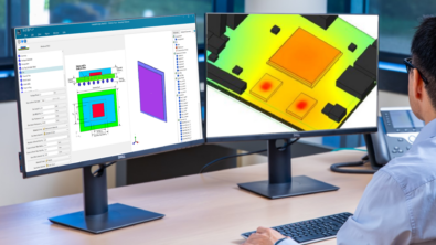
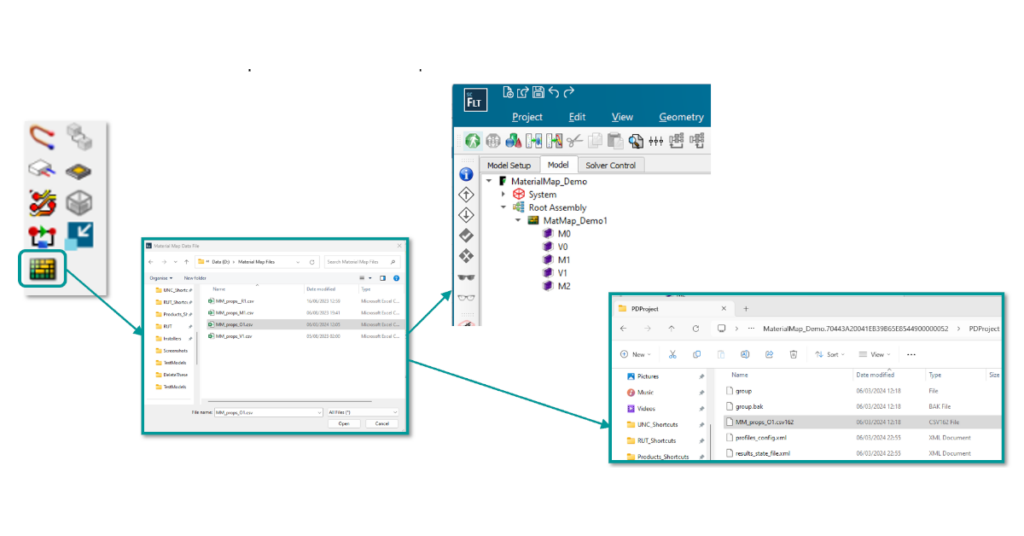
To create, users select a new SmartPart Icon that opens the file selection dialog. Select the file and the Material Map SmartPart is created in the Root Assembly Tree:
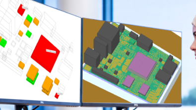
Watch this video demonstration below to learn how to use the Material Map SmartPart and how to import a Material Map text file into a PCB thermal analysis workflow. For maximum accuracy a fine resolution of the PCB is needed to match the accuracy of the detailed semiconductor package model to accurately capture the connection between the package and the copper traces. This workflow illustrated features a PYTHON scripting utility for the creation of the Material Map from images in an ODB++ file. Subsequently, the steps to import the board via EDA bridge for component placement and assigning powers are explained, before implementation of the Material Map Smart Part and localized modeling configuration for copper and layer modeling are demonstrated.
You can see that for that a Material Map Smart Part that it can be placed, rotated, mirrored and aligned as an object within a Simcenter Flotherm model while the size is strictly fixed as it is defined within the Material Map file imported. A material map region cannot be manipulated as these are set in the file details also, however you can align other objects and SmartParts with regions to facilitate system level modeling tasks.
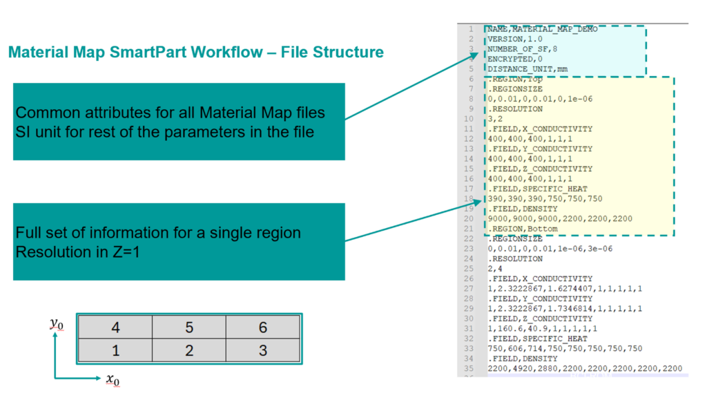
Understanding a Material Map File Structure
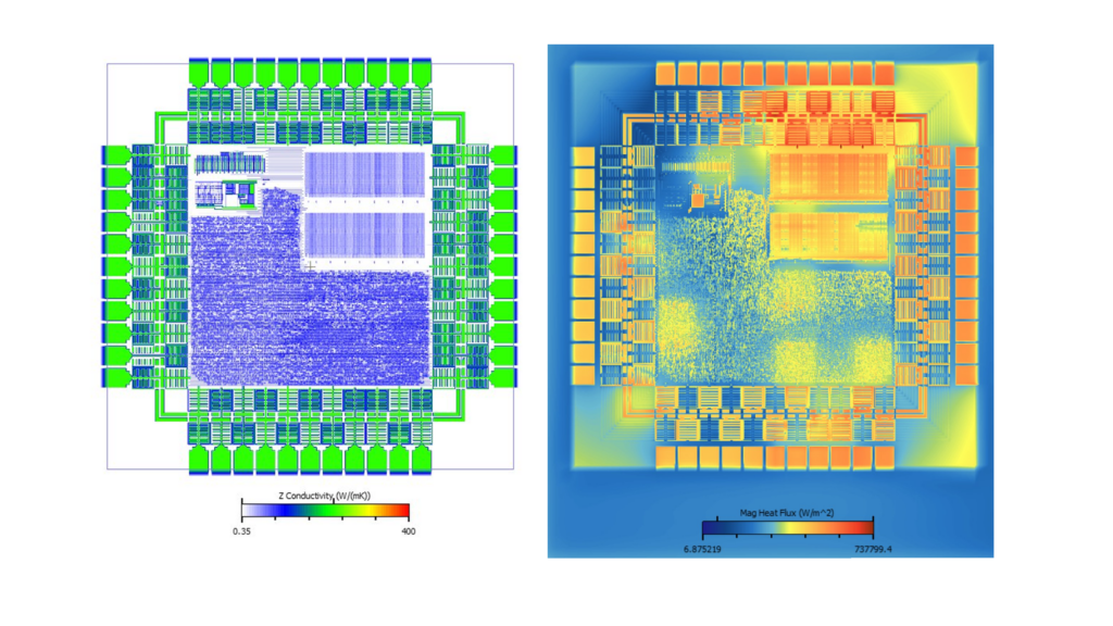
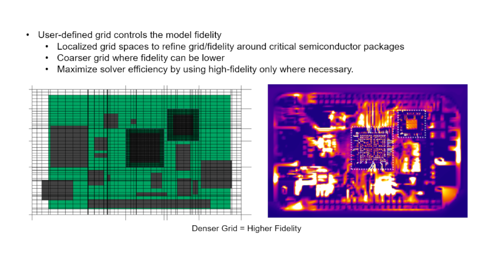
Localized modeling fidelity control via gridding
The maximum resolution of the material map will be defined by the data in the file imported. The recommendation is to use as high a resolution as possible in this file when generated and to then control the resolution in the model set up using Simcenter Flotherm grid controls . A coarse grid where resolution can be low, and a fine grid to target accuracy around critical semiconductor packages is recommended for optimal solver efficiency. Underlying technology will use the data supplied to apply the appropriate effective material properties into each grid cell.
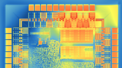
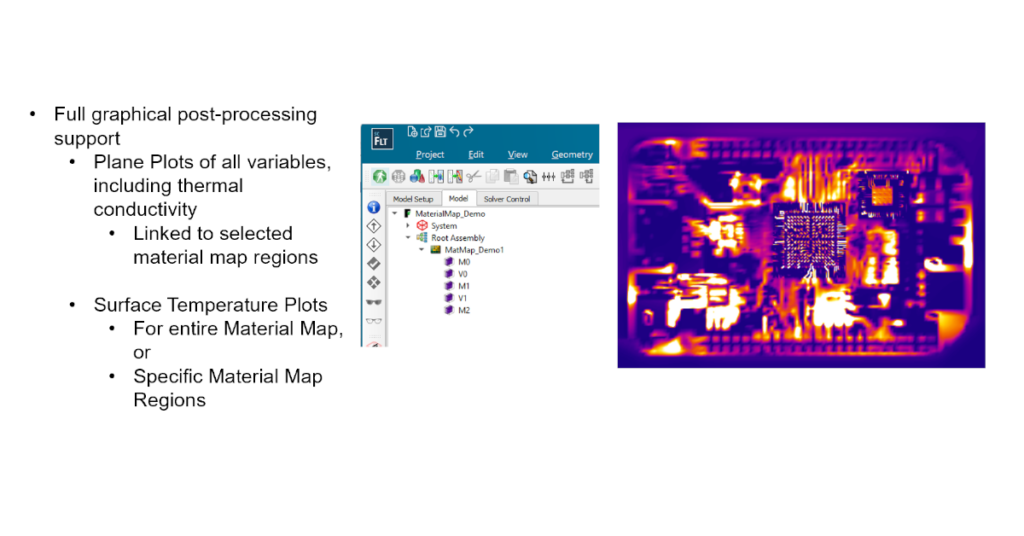
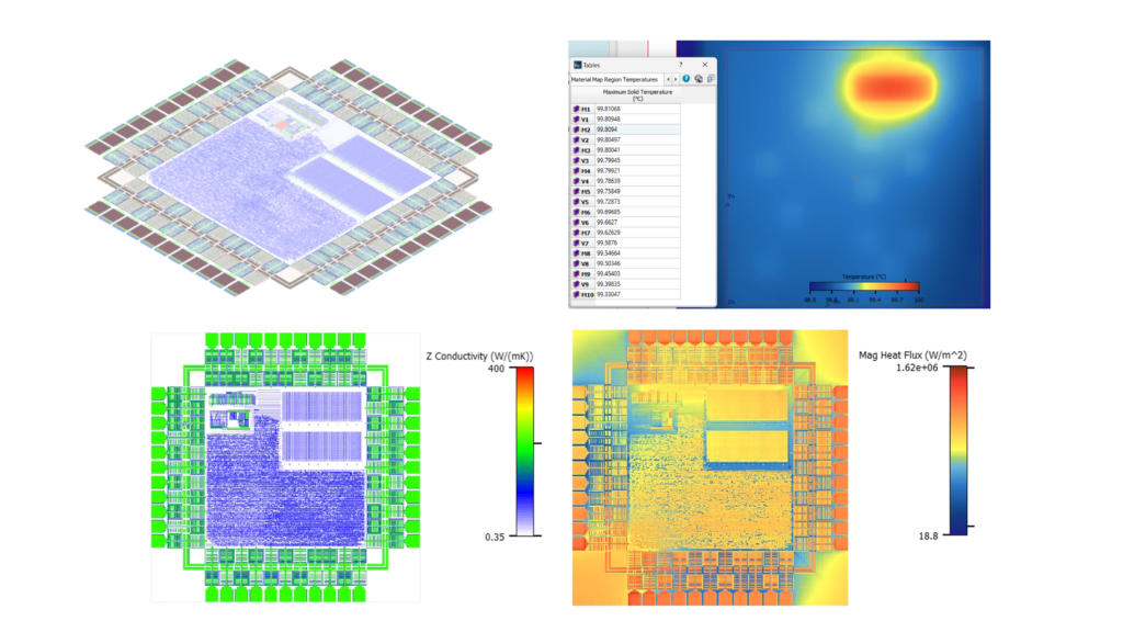
Post-processing – viewing results
For a material map SmartPart there are tabular temperatures available. For individual regions fluxes and temperatures are in tabulated form.
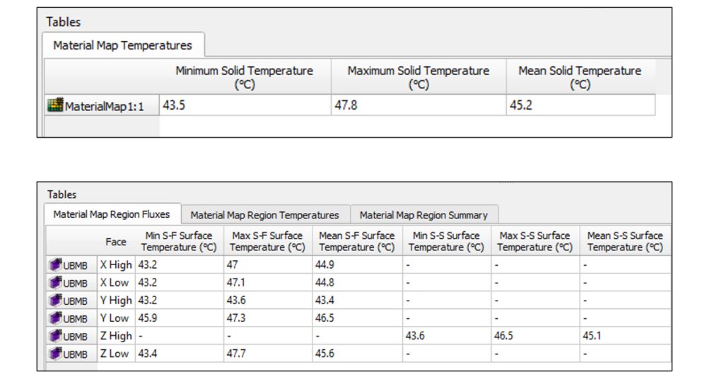
For plane plots and cut plots there is comprehensive graphical user interface support.
Faster thermal analysis performance
The Material Map SmartPart computational efficiency is reflected in model loading and translation time when compared to typical explicit modeling of geometry and materials. Below are 2 examples of the indicated faster loading and translation processes in the order of 10 times or to over 1000 times faster , which can positively impact overall analysis processing time.
There is also significant speed up in selection and post-processing operations. In the case of temperature plots and plane plots, these are 7-9 times faster to perform which adds value especially when post processing batches of simulations. Simcenter Flotherm software is continually incorporating developments that enable users to shorten thermal design time and preserving accurate analysis.
IC package thermal modeling
With increasing complexity of IC packages, it is advantageous to have highly accurate, yet computationally efficient, representation of detail in substrates, interposers, and die metallization. This is especially important in the design of 2.5D and 3D multi-die package applications where complex structures and heat flow paths require careful thermal management to avoid issues with device performance, behavior, and reliability. Modern package architectures enable the flexibility to arrange chips, or chiplets, in 3D space. Such chiplets may be arranged side-by-side or stacked with high numbers of possible combinations to evaluate for thermal behavior.
Leveraging Siemens EDA software in conjunction Simcenter Flotherm, semiconductor companies are able to develop accurate detailed 3D thermal models and then generate 3D reduced order thermal models that are secure and shareable with downstream clients in the electronics supply chain.
Watch the following video to see how the Material Map SmartPart is used in a detailed IC package thermal model for thermal analysis. The model in this video below is imported from Calibre 3DThermal, a new thermal analysis tool for IC Designers that leverages Simcenter Flotherm technology. The video then shows how an Embeddable BCI-ROM model of the package can be generated in Simcenter Flotherm, which is then possible to share securely for surface temperature and internal temperature prediction in 3D CFD electronics cooling analysis studies.
Video: IC package thermal models to system level modeling CFD across the electronic supply chain
Where to find out more.
For users , you can download Simcenter Flotherm 2404 now on support Center now available as of April 10th, 2024. Release highlights documents and release notes are also found on Support Center.
If you use Simcenter Fotherm as a thermal engineer, or your company uses Calibre design tools for IC Designers from Siemens EDA, including Calibre 3DThermal, then please contact your account contact, Siemens pre-sales engineer or support engineering team. We welcome opportunities to explore ways to improve IC design flows and specifically enhance IC package thermal modeling throughout development to shorten your processes.
If you are not using Siemens tools today or do not have your Siemen account manager contact details, please contact Siemens
If you are a IC designer or architect looking for an overview of key reasons for adopting robust multi-discipline design capabilities for successful 3DIC development, please see this blog. If you want to find out more about Calibre 3DThermal, a tool for thermal analysis for IC Designers please visit this page.