Key Thermal Advances Driving Next-Gen AI Chip Design in 2026
AI is hot — literally.
As we bid farewell to a transformative year of 2025, there’s no doubt that the AI chip underwent substantial changes. As AI compute is pushing into unprecedented power levels, thermal management emerges as the new bottleneck for reliable system performance.
The shift to 3D chip architecture only amplifies this challenge: stacking heterogenous dies in a compact space leads to higher power density, creates intense localized hot spots and, traps heat in tiers far away from the heat sink. If you’re wondering just how extreme it gets: power densities in leading-edge 3D ICs have already been compared to the surface of the sun. That’s the uncomfortably “hot” reality every AI hardware designer now must confront.
As 2026 ushers in new advances across materials, packaging, AI, and multiphysics simulation, here are five thermal trends to watch and how they’ll reshape design and packaging workflows.
#1 Cooling will start inside the silicon
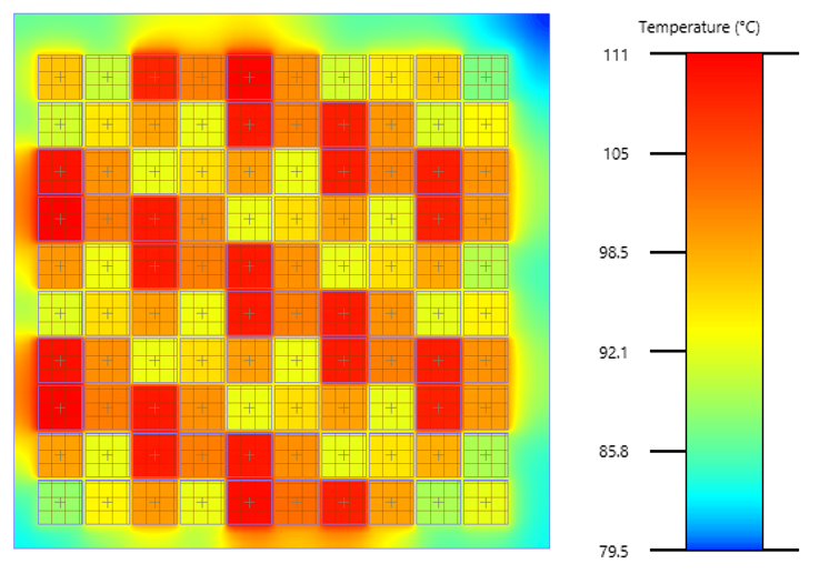
With GPUs racing toward kilowatt-class thermal design power, today’s direct-to-chip (D2C) conduction-based cooling approaches will soon hit their practical limits as they can only extract heat from the top surface of the die. To improve thermal reliability for next-gen 3D IC systems, researchers have been exploring microfluidic cooling by etching microchannels directly into the silicon or interposers. These channels function like a engineered “circulatory system,” routing coolant just micrometers from active transistors. Many proposed implementations use two-phase cooling, where the coolant absorbs significant heat during liquid-to-vapor phase change, dramatically reducing thermal resistance and improving temperature uniformity across tiers.
However, this innovation brings a major increase in modeling and simulation complexity. Once cooling gets embedded inside the die, it becomes an active architectural design element itself. Engineers will need highly accurate 3D geometric representations of micro-channel networks, multiphysics solvers that can handle both single- and two-phase flow, and tightly coupled analysis across power delivery, routing, and thermo-mechanical stress.
#2 Beyond CoWoS: System-on-wafer integration is here
Industry roadmaps for AI systems are quickly moving beyond today’s CoWoS towards full System-on-Wafer (SoW) integration, to cut costly off-chip communication by placing compute, memory, and accelerators across an entire wafer. For instance, TSMC plans SoW-X by 2027, integrating up to 16 compute dies and 80 HBM4 stacks.
But wafer-level integration also introduces a new level of thermal complexity: a naïve finite-element thermal simulation of a full wafer would require billions of mesh cells, exceeding practical solver runtime.
That’s where a hierarchical thermal analysis solution will become paramount. Engineers can perform detailed simulations on small blocks such as chiplets, tiles, and local structures; those results are then distilled into reduced-order thermal models; and finally, system-level solvers combine these models into a full-wafer analysis.
#3 New thermal interface materials emerge for 3D ICs
Thermal interface materials, TIM1 (between the die and heat spreader) and TIM2 (between the lid and heat sink), remain one of the most stubborn thermal bottlenecks in 3D IC packages. TIM1 is especially critical because it sits closest to the silicon. An ideal TIM needs to transfer heat effectively across interfaces while maintaining their mechanical integrity.
Currently, indium foils are among the most promising choices for TIM1 in high-performance packages. To facilitate even better thermal transfer, researchers are exploring various advanced materials, including phase-change materials (PCMs), highly conductive solids like graphene sheets and copper/carbon nanotube structures, high-performance thermal gels (such as silver-filled gels), and liquid metals. Some novel approaches attempt to eliminate the TIM materials overall by additively building advanced cooling structures on the die itself.
#4 AI will play a more crucial role in thermal analysis
Brute-force thermal simulation becomes infeasible for future wafer-scale AI systems; resolving every layer down to the transistor level exceeds compute budgets. EDA vendors are increasingly turning to AI-assisted thermal analysis.
One of the applications is intelligent design space exploration. Engineers can parameterize the variables that drive temperature behavior—materials, floorplan, microchannel geometry, boundary conditions, and TIM properties—and let AI automatically generate and simulate hundreds or thousands of model variants. By analyzing how each parameter affects junction temperature, thermal resistance, and hot-spot formation, AI (through advanced optimization algorithms) helps identify the dominant factors so that engineers can focus on the true thermal bottlenecks.
#5 EDA will redefine how designers and thermal engineers work together
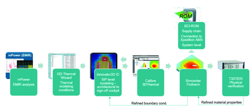
Ensuring thermal, power, and mechanical reliability is an inherently interdisciplinary problem — one no single innovation in chip architectures, TIMs or cooling designs can solve in isolation. The future of scalable 3D IC designs will depend on our ability to co-innovate across IC design, advanced packaging, material science and manufacturing. What’s emerging is a new design culture where electrical, mechanical, and thermal engineers work from a common digital thread from design planning to manufacturing tests.
Siemens is enabling this shift through fully connected die-to-system workflows. For example, Innovator3D IC Integrator establishes the authoritative structural and assembly model, while Calibre 3DThermal converts that layout into a high-fidelity thermal model that seamlessly feeds into Simcenter Flotherm for system-level analysis. This and similar digital threads help engineers of various backgrounds leverage the same multidisciplinary (electrical / thermal / mechanical) digital twin across design teams.
2026: The Turning Point for Thermal
2025 was the year AI chips got hotter.
2026 will be the year we learn to cool them smarter.
With the rise of 3D ICs, wafer-scale integration, and kilowatt-class AI accelerators, thermal is no longer something you “check at the end.” The teams that stay ahead in the AI hardware race will be the ones who bring thermal insight into every design decision.
At Siemens, we’re building multiphysics-aware, die-to-system design flows that give engineers early visibility into thermal interactions. If you’re rethinking your design flow to handle emerging thermal challenges, we’re here to help you evaluate alternatives quickly, spot issues early, and design with confidence.


