PCBflow helps make your innovative vision a reality by re-imagining the electronics design-to-production process.
In the rapidly evolving landscape of electronics manufacturing, staying ahead of the curve requires embracing innovative tools and technologies. One…
I love a good story. Storytelling is the new, cool skill to list on your CV, but listening is possibly…
Design for manufacturing, or DFM, is a crucial aspect of electronics manufacturing best practices. It emphasizes that each printed circuit…
One of the biggest challenges in the process of a design to manufacturing handoff is the lack of manufacturing knowledge…
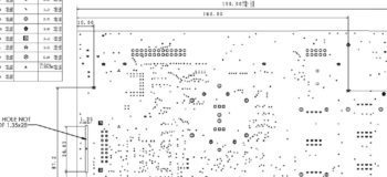
A silkscreen contains human- and machine-readable marks on the surface of a PCB that indicates PCB components’ positions and polarity,…
On an August evening in the sky above a California desert, a skydiver leaped from the safety of an airplane…
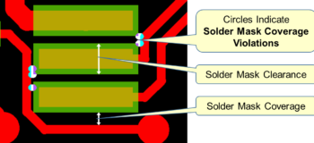
In the realm of PCB fabrication, it is commonplace for manufacturers to “tweak” board designs provided by designers in order…
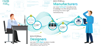
Shift left – Shift Right (1st part out of two) In 1887 the great city of Chicago in response to…
The Gerber data transfer format has been serving the PCB manufacturing industry for decades, and the Extended Gerber standard (also…
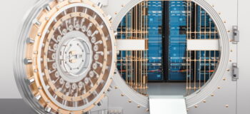
A look at how PCBflow keeps your board design and manufacturing capability files secure
A majority of PCB fabricators proudly publish their aspect ratio production capability. Some even go further and publish their maximum…
Siemens’ collaboration space for connects electronics designers and manufacturers to shorten the design-to-production process
During my years in the PCB pre-production world, I’ve seen the challenge of preparing design data for production in a…