PCB Aspect Ratio – how do you know your board is manufacturable?
A majority of PCB fabricators proudly publish their aspect ratio production capability. Some even go further and publish their maximum aspect ratio per hole type, which is especially important for high density interconnect (HDI) boards. But how can you be sure that your design meets your manufacturer’s PCB aspect ratio capability?
What is PCB Aspect Ratio and why is it important?
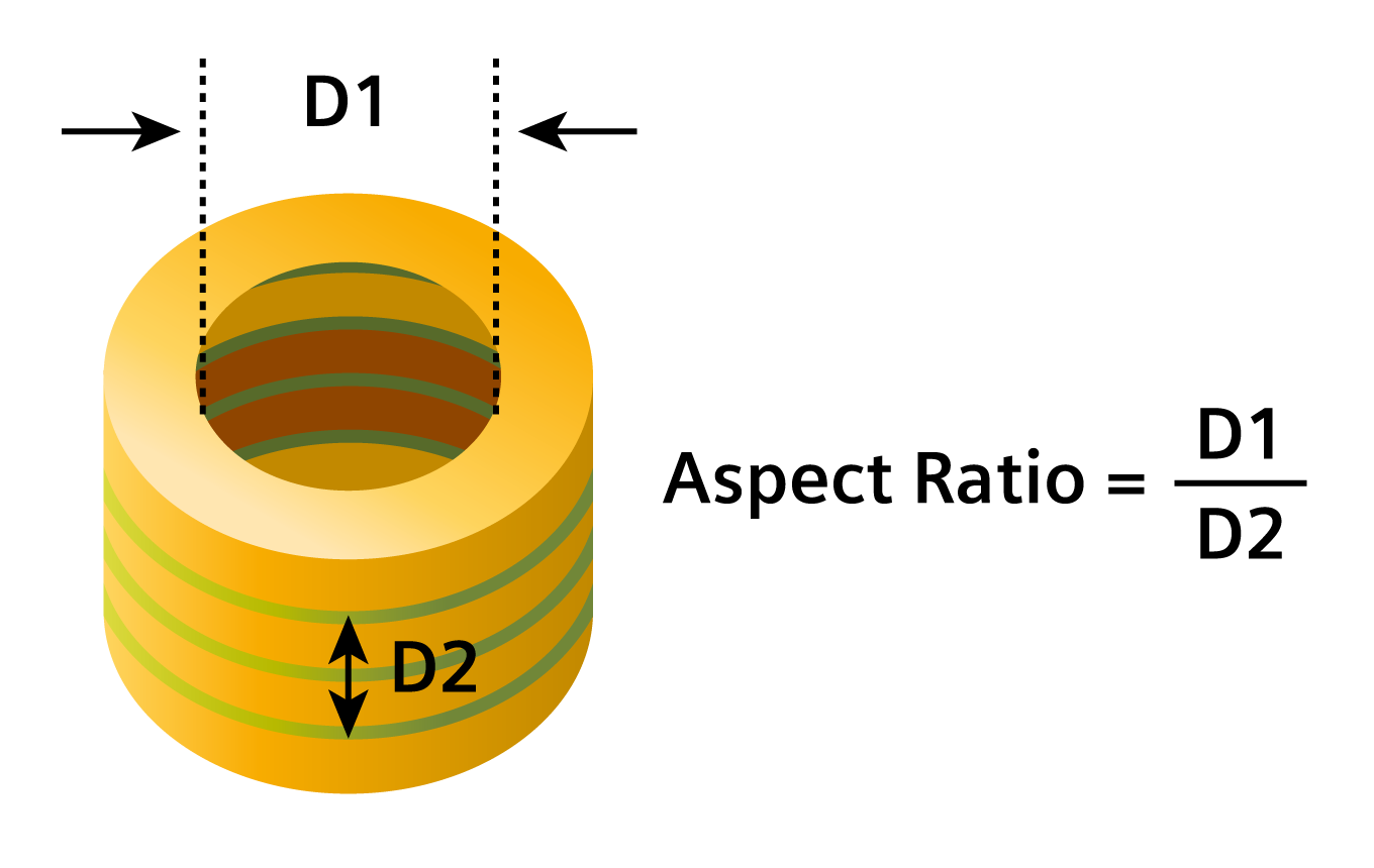
Aspect Ratio is the ratio of the hole’s diameter to the thickness of the material it is piercing through, as shown in figure 1:
Figure 1: Aspect ratio
Aspect ratio is particularly critical for ensuring a consistent plating process: the smaller the aspect ratio is, the higher the probability of consistent copper plating throughout the length of the hole. Aspect ratios that are higher than the maximum supported by a fabricator may result in insufficient plating of the hole, which, in turn, will result in a broken net in the case of a via hole, or in assembly failure in case of a component plated through-hole.
Fabricators usually publish a set of maximum manufacturable aspect ratios for multiple processes, such as through holes and microvias. And of course, each fabricator may publish a different set. With all this uncertainty, it is very important to verify that your design is suitable to your manufacturer’s capabilities in general – and to their aspect ratio in particular.
So how do you verify it?
Usually, the aspect ratio is checked by the manufacturer as part of the DFM process. But here’s the challenge – both the designer and the manufacturer are missing crucial information:
- While the hole’s diameter can be obtained from the design data, the board thickness and material (copper and dielectric) thickness values are not included in the Gerber data – as they are not part of the format — and are usually delivered in the documentation or in a drawing. So, in order to properly verify the aspect ratio, these values should be communicated to the manufacturer. Unfortunately, this is a manual process, and is prone to error.
- You, as the designer, may not know the relevant aspect ratio capability of your manufacturer, and the resulting uncertainty may result in additional, resource-consuming design spins. Can they be avoided?
The PCBflow Solution
PCBflow was designed to eliminate aspect-ratio uncertainty: When you run DFM checks against your manufacturer’s capabilities, you can safely assume that their relevant aspect ratio values are set correctly. And when you upload your design in ODB++Design format to the manufacturer, all thickness values are in the file – for both through holes as well as for blind and buried vias.
While PCB Aspect Ratio is highly important, it is only one of the hundreds constraints PCBflow reviews.
PCBflow runs in a secured cloud environment, so you can rest assured that your IP is fully protected.
Sign up and try it out at https://www.pcbflow.com/.