Solder Mask Coverage Violations and how to prevent them
During my years in the PCB pre-production world, I’ve seen the challenge of preparing design data for production in a way that is both cost-effective and will improve production yields. Most PCB fabricators agree that if PCB designers would take into consideration the fabrication constraints and their impact on the fabrication process, they would be surprised at how easy it could be to improve their designs.
Solder mask preparation is one of the bigger challenges in this field, and solder mask coverage provides an excellent example of the impact that design practices have on successful fabrication.
Let’s have a look!
Solder Masks and Clearances
In order to protect the copper traces of a printed circuit board (PCB) from the environment and from undesired electrical contacts (solder bridging) during assembly, a thin, non-conductive layer called solder mask (SM) is applied to the outer layers of the board. After the mask is applied, openings in the solder mask – known as clearances – must be created wherever components are going to be soldered. Those openings are defined in the SM layer on each side of the board and taken into consideration during all stages of PCB design, fabrication and assembly.
When analyzing a board for manufacturability, special attention needs to be paid to the solder mask, since faulty clearances may result in assembly process defects, which, in turn, will result in the scrapping of assembled boards, and in reduced project profitability.
What is an “SM Coverage Violation”?
Solder mask clearances should be large enough to securely expose copper pads for soldering. On the other hand, they should be small enough in order to keep away from copper traces or other copper features that should not be exposed. In dense designs, these two requirements often contradict, requiring layout engineers to compromise and optimize.
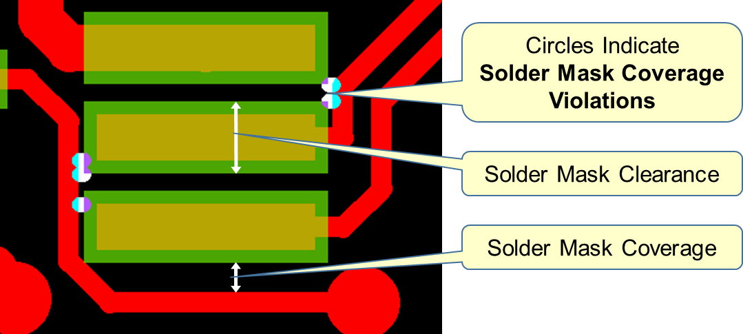
The distance between the solder mask clearance and the unexposed copper is called “SM Coverage”. An example appears in the figure below.
When insufficient SM coverage exists – in which the SM clearance is closer to unexposed copper than specified in constraint values – this is considered an “SM Coverage Violation”, which requires the attention of the layout engineer.

In addition to layout considerations, PCB fabricators need to consider the potential inaccuracies caused during the photo-lithographic process used to create SM clearances after the solder mask is applied. These inaccuracies might cause solder mask clearances to slightly change their shape and/or location. Thus, during PCB fabrication analysis, a minimum SM coverage distance is set as a constraint parameter – this parameter must be set in accordance with the procedures employed by the fabricator.
Why it is important to detect SM coverage violation in the early stage of layout?
When a SM Coverage violation is detected during a pre-production fabrication analysis, the usual procedure is to reshape (shrink or partly shave) the faulty clearance in order to increase the distance between the clearance and the exposed copper. Besides being tedious and error-prone, this process compromises the clearance quality.
If these violations are detected early in the design process, the layout engineer can more easily remediate them. This is where PCBflow comes in. PCBflow is Siemens’ online DFM (Design-for-Manufacturing) tool . Developed for use by board designers in startups and SMEs, PCBflow provides immediate feedback on design errors and violations, thereby reducing the number of board spins which can cut costs and reducing time-to-market.
PCBflow issues alert indications when errors or violations occur. For example, it provides notifications of SM coverage violations in the layout stage, allowing the layout engineer to find an optimal solution – for instance, by using thinner traces, or by rerouting the traces away from pads.
The platform runs in a secured cloud environment, so you can rest assured that your IP is fully protected.
Sign up and try it out at www.pcbflow.com.