Your blueprint for next-gen 3D IC success

In today’s semiconductor landscape, traditional scaling approaches are hitting physical and economic limits. The industry is pivoting toward 3D IC technology as the path forward, with over $200 billion being invested in advanced fab capacity for AI and HPC chips. With the global semiconductor market expected to double to $500 billion by 2030, here’s your roadmap to 3D IC next-generation success.
Embrace heterogeneous integration as your foundation
Heterogeneous packaging represents a critical inflection point in semiconductor design. This approach:
- Combines different technologies (logic, memory, analog) in a single package
- Overcomes Moore’s Law limitations without relying solely on transistor scaling
- Optimizes power, speed, and thermal management in advanced applications
- Enables critical functionality for AI, 5G, and high-performance computing
As Bryan Black, CEO of Chipletz, notes:
We selected advanced design tools as they demonstrated their technologies’ capability and capacity, along with their expertise in advanced heterogeneous semiconductor package design.”
Implement a system-centric design approach
Success in 3D IC requires thinking beyond individual components:
- Adopt system-level design, partitioning, and optimization
- Utilize virtual prototyping to evaluate design scenarios early
- Implement heterogeneous system co-design across die, interposer, package, and PCB
- Apply a “shift-left” approach to prevent costly downstream rework
Suk Lee, VP & GM of Ecosystem Technology Office at Intel Foundry, emphasizes:
For advanced heterogeneous integration platforms such as EMIB, an integrated floor planning and prototyping cockpit with predictive analysis is essential.”
Prioritize early multi-physics verification
Thermal and mechanical challenges intensify with 3D integration:
- Conduct predictive SI/PI/Thermal modeling early in the design process
- Implement integrated heatsink design and thermal solutions
- Perform comprehensive interference checks between ECAD and MCAD domains
- Utilize computational fluid dynamics (CFD) analysis to optimize thermal performance
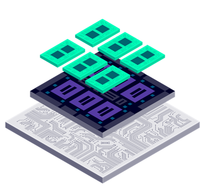
Accelerate innovation through chiplet-based design
Chiplet architecture provides key advantages:
- Mix and match different geometries and foundry technologies
- Avoid reticle limitations of single-die approaches
- Reduce costs and improve yields compared to monolithic solutions
- Enable high-bandwidth, low-latency connections between components
Ensure manufacturing success
Design excellence must translate to production excellence:
- Make early DFM/DFY/DFT implementation critical during package design
- Focus on scalability for mass production
- Establish clear verification and sign-off processes
- Maintain digital continuity from concept to manufacturing
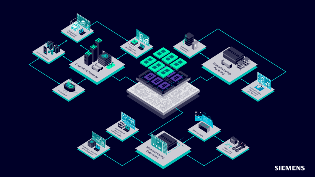
Leverage standards and ecosystem collaboration
No company can succeed alone in the 3D IC era:
- Implement Chiplet Design Exchange (CDX) standards to drive innovation
- Reduce complexity through standardized interfaces
- Collaborate across the ecosystem with foundries, OSATs, and design partners
- Utilize comprehensive multi-physics design flows and verification tools
The path forward
The shift toward integrated, software-centric solutions enables semiconductor companies to create flexible, intelligent products that open new revenue streams. By following this blueprint—embracing heterogeneous integration, implementing system-centric design approaches, prioritizing early verification, leveraging chiplet architectures, ensuring manufacturing success, and fostering ecosystem collaboration—you’ll be well-positioned for success in the 3D IC next-generation era.
Explore our 3D IC design solutions to help you achieve faster time-to-market for semiconductor products.