From disconnected systems to digital traceability: a digital thread from design to manufacturing

As a child, did you ever use building blocks to create something original? It may not have been stable, but you likely enjoyed the time spent building something new. Today you can buy kits with all the right pieces and instructions to help you build exactly what you see pictured, ensuring structural integrity and reducing hours spent on guesswork.
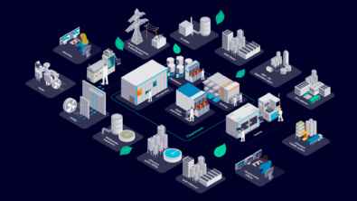
Similarly, the semiconductor industry’s history with legacy and homegrown systems are not built with the scaling needed to meet today’s industry expansion and complexity. These fragmented systems are unconnected without a common data platform or language and require too much of our time to work within them. Design and manufacturing teams do not have the benefit of seamless data flow from the design, planning, processing and reporting phases that empower collaboration and true innovation.
Taking control of product data and processes for true digital transformation
As a result, design engineers waste time trying to find the information they need and potentially convert it into a format they can use. For semiconductor companies to keep up with the current pace of innovation, taking control of their product data and processes is critical. The first step is committing to build a single product lifecycle management (PLM) platform to store, access, share and manage data throughout the product lifecycle and across the value chain. To achieve this goal, they must include EDA design and verification, packaging design data, embedded software, documentation, bill-of-information (BOI) data and bill-of-process information (BOP).
True digital transformation begins with lifecycle management that connects all systems and objects to provide one continuous digital thread of data throughout the entire manufacturing process from end-to-end while also providing the ability to store, access and manage all data.
Without all the information it would be impossible to harmonize all design and manufacturing process information for the entire lifecycle of the product. The result is a holistic view of all the product design, manufacturing and process data from across the enterprise that ends fragmentation.
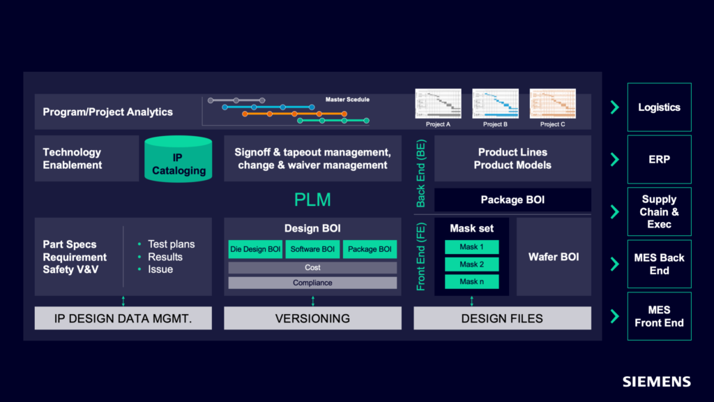
The PLM ecosystem diagram below shows some of the different modules for the semiconductor solution and its design integration touchpoints, including version control systems, design simulation and verification EDA tools, plus the IP design data management system, manufacturing execution system (MES), logistics and supply chain data.
With such comprehensive, detailed information flowing within the enterprise, a semiconductor company can expect to improve reliability, achieve faster new product introductions (NPIs), reduce design re-spins and costs and provide secure supply chain collaboration. The overall result? Increased innovation and better product quality.
Product complexity is driving accurate lifecycle traceability reporting requirements
Alongside increasing product complexity you’ll find traceability requirements. Manufacturers need deeper insights to ensure end-to-end traceability of components and systems. With PLM, a lifecycle traceability report for a product revision shows how digital and physical assets are connected, creating a single digital thread from design to manufacturing. These detailed reports provide real-time information for root-cause analysis, IP revision identification, and more.
Learn more about how chipmakers can achieve end-to-end traceability and maximize product quality in the new ebook.