fabricator etching a PCB

Etch effects exposed: discover where your copper really goes

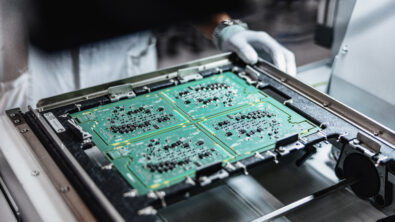
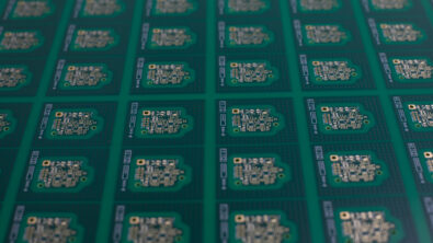
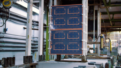
Etching inner layers involves cleaning the copper on both sides of the piece of laminate, applying a photoresist, exposing the photoresist to create the inner layer pattern, developing the resist, etching away the unwanted copper, and removing the etch resist. This process is automated in most shops and the chemistry is automatically monitored. As a result, the accuracy and repeatability is quite good. It is possible to etch inner layer traces using this process to an accuracy of ±0.5 mils. This accuracy control helps keep impedance within the tolerances required for transmission lines.

what's new in Z-planner 2510

What’s new in Z-planner Enterprise 2510

The Z-planner Enterprise 2510 release of Z-planner continues to refine the product by focusing on simulation accuracy, overall ease of use and collaboration.

dielectric material loss

Cutting your losses – loss planning and you

Loss planning – What is the best laminate for a loss budget of x dB for y inches?  I was thinking in terms of Panasonic Megaton (sic) 6 or something like it.

copper thickness in PCBs

Copper thickness: Closing the knowledge gap to design success

Copper thickness determination of rolled and electro-deposited (ED) copper foil by weight provides far more accuracy than contact-thickness gauges. Since the topography of treated foil varies greatly, and since the density of copper is known, weighing a 1-by-1 foot sheet is the best way to determine the average thickness of a sheet of copper.  So formally, the unit that we refer to as “ounces” is actually ounces per square foot.

What's new Z-planner Enterprise 2504

What’s new in Z-planner Enterprise 2504

Z-planner Enterprise 2504 release The latest 2504 release of Z-planner Enterprise delivers powerful updates that streamline stackup planning, improve rigid-flex…

Crosstalk along traces

Your #1 defense against a crosstalk crisis

It’s been some time since I’ve seen an article on crosstalk, so I decided to take the opportunity to walk…

PCB material selection for PCB stackup design

Avoid overspending on stackup materials in your PCBs – 8 high speed materials to consider

PCB material discussions are often focused around stackup material selection. These tend to be framed by questions like: ‘We use material ‘x’ for our designs and really like it. What do you think of it?’ This often veils the real question which is: ‘Do you know a good alternative to it?’

What's new in z-planner 2024.1

What’s new in Z-planner Enterprise 2409 – stackup design wizard, impedance, compare stackups, DFSI

What’s new in version 2024.1 of Z-planner Enterprise including information on the enhanced stackup design wizard, impedance tab, compare stackups, improved import/export, DFSI and more

PCB DFM fabrication

4 things a PCB librarian needs to know about PCB fabrication

a PCB librarian also needs to understand how the PCB is going to be built by a PCB fabrication factory. The PCB fabrication process involves dozens of steps, which can often be more complicated than the PCB assembly process.