PCB stackup

On-demand webinar: PCB Stackup Planning

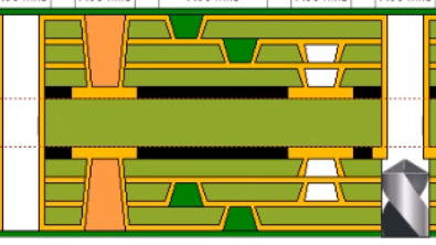
See how material choices can make or break your design, and how to compare materials not just for the technical match, but for selecting the best material at the best value. You will also learn how today’s (and tomorrow’s) high speed circuits have brought new considerations into stackup design such as copper surface roughness and glass-weave skew.

Online PCB DFM

Smart Design-to-Manufacturing Handover with Online PCB DFM

PCB design handoff needs a solution PCB design is more complex than ever before, and at the same time, designers…

NEPES partners with Siemens to streamline its advanced wafer-level IC Packaging wafer map mask creation process

NEPES partners with Siemens to streamline its advanced wafer-level IC Packaging wafer map mask creation process

Siemens’ Xpedition Package Designer automates a manual error prone process saving days of effort and reducing risk Seoul, South Korea.,…

Benefits of cloud based pcb dfm

PCB Cloud Based DFM – Why You Should Care

The Covid -19 pandemic has been a reality check for organizations of all sizes. Due to these uncertaintimes, more organizations,…

PCB manufacturer: Collaborate with design houses while securing your intellectual property

How to make sure that your manufacturing process capabilities remain private, even when shared with others Background Siemens presents a…

Copper layers on PCB

Old Habits Die Hard

In one of my previous blog posts, I asked the question: Why do designers keep sending Gerber files to their…

What’s New in HyperLynx® – VX.2.8

Check out what’s new in the latest VX.2.8 release of HyperLynx – the industry’s complete family of analysis tools for…

Mentor Communities Have a New Home!

Mentor communities are now fully integrated with the Siemens Digital Industries Software communities. This integrated PCB Systems Design community experience…

PADS Professional VX.2.8 is Now Available!

The new release of PADS Professional VX.2.8 is now available for download.