Layout automation using advanced PCB design techniques – Part 2
In part 1 of this blog series we started the PCB design process by looking at part placement automation.
Let’s move on to constraints. Many designers try to avoid the constraint management process except for the basics as they find it time consuming and difficult. However, constraints are the backbone of good PCB design. Without constraints it’s difficult to produce a design that’s correct 100% of the time especially when the design is anything but simple.
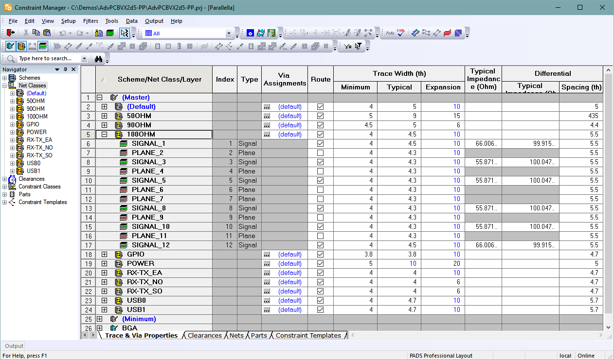
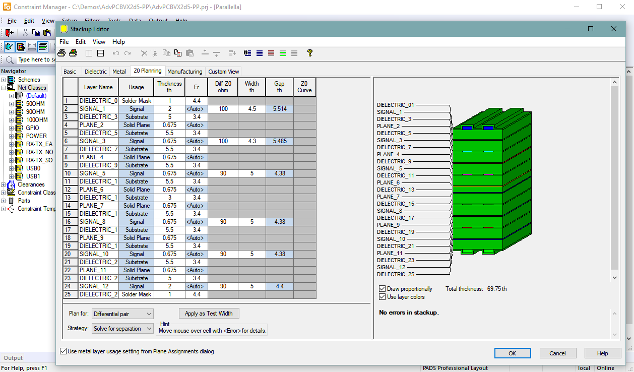
PADS Professional provides a constraint editor system that allows you to define all the rules that most feel are overly complex in a simple and structured fashion. Let’s start with Net Classes. Why is the process of creating net classes worthwhile? Classes allow us to organize groups of nets that require the same physical rules. Rules defined on a net-by-net bases will become very unorganized and difficult to manage. Classes provide additional benefits like: assisting with viewing, setting colors, design review, using routing automation, etc. In our example design shown in (Figure 1), we have 10 Net Classes defined. The 100, 90, and 50 Ohm classes allow us to define trace width impedance rules based on layer, simplifying routing. With CES we also have access to HyperLynx stack-up editor which allows us to determine single-ended and differential pair trace widths and gaps for impedance controlled nets (Figure 2).
From the Zo Planning tab we can find the proper trace width and the tool will calculate the gap. Trace width and gap will automatically adjust depending on the layer its routed on, plus you can control which layers will be used for routing. These classes could have been made more granular by doing it based on specific net groups, this a decision you will make based on design requirements.
Note: using an environment like CES in PADS Pro provides simple copy/past and drag/drop replication to speed the process of defining values for multiple objects.
The one thing we have not defined yet are our physical spacing rules between objects. Our net class definition only created a container for a group of nets, the routing layers, trace widths by layer, and differential pair trace width/gap. Every design contains certain technology or requirements that use specific clearance rules but not every net group needs these special rules. With most tools you define physical spacing rules with a net class. This makes the process simple but it does not really allow you to define different spacing rules between classes very easily.
Typically, more complex and time consuming processes are required to define class to class spacing rules. With PADS Pro we have a special section for Clearances which allows you to define specific rules based on technology or requirements (Figure 3). This is where rule reuse comes into play. Once the general and special clearances have been defined we use a simple class-to-class matrix to define where our spacing rules will be used. The power here is if a clearance requirement changes you don’t have to remember where those rules where set. We just change the clearance group in question and it’s automatically applied where needed (Figure 4).
Download a free trial of PADS Professional today!
What happens when you work on that design with a new processor, DSP, or FPGA were the package is only available in .8mm or smaller pitch package? Or what if you’re introducing RF circuitry like 5G or designing products with high voltage? With most design tools you need to be cognitive of where traces traverse boundary’s requiring different trace width and spacing.
To simplify our design process we could use rules that are specific to an area of the board. When this capability is needed it by far outweighs most anything else that would save us time when routing our design. With PADS Professional this capability is called “Area Rules” and is defined in CES using Schemes. Schemes automatically adopt all Net Class and Clearance groups whether new or already created. As a designer you now have the capability to redefine trace widths and clearance requirements for a given scheme (Figure 5).
Now that we’ve created the core rules required to design a PCB. What if we have nets sensitive to signal quality, like SerDes differential pairs, DDR, common interfaces like USB, Phy, HDMI, etc. These all require special electrical rules like: length matching, special vias, topology control, trace length control by layer, maximum via count and differential pair creation. In some rare instances the need to create rules that rely on length information from other nets or pin pairs may be required to simplify routing.
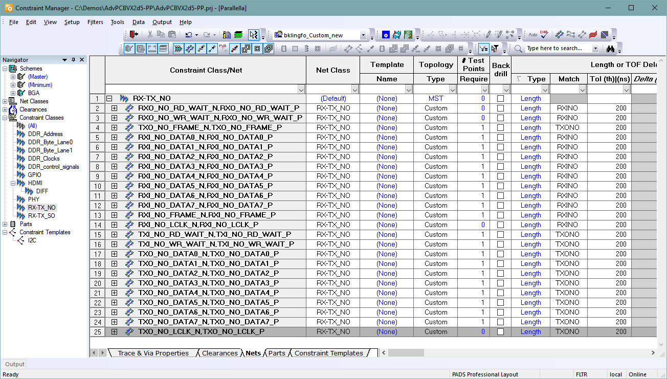
PADS professional provides this capability with the use of formulas. All these types of rules are classified in CES as Constraint Classes (Figure 6). Why a “Class”? Because each grouping you create will include net assignments similar to net classes. One might also ask “I’ve already created net classes why do i need to do it again for length rules?” The reason is Net classes define spacing and trace width requirements which would allow you to combine nets that may not have the same electrical rule requirements. This can all be clarified with an example. Let’s say we have differential pairs that need to be 100 ohms and we’re not concerned about layer restrictions. These nets could include SerDes, DDR Clock and Strobe, HDMI, etc. When it comes to electrical rules all of these would require their own classes, but we can simplify trace and space rules by putting them in the same Net class.
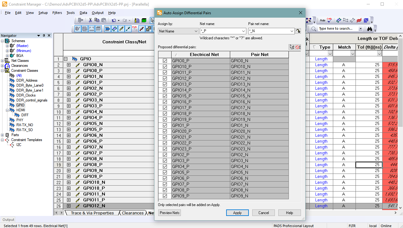
Let’s talk about differential pairs in a little more detail as these are probably the most common special rule feature we might use in a design. Whether you’re in the schematic tool (Pro Designer) or layout (Pro Layout) we can access the same CES system with all the same rules including creating pin pair definitions and differential pairs. CES provides automation to help you create your diff pair associations so you’re doing each net pair one at a time. Assuming we’ve done our schematic correctly and named diff pair nets with a proper suffix (ie. _P and _N) or something to that effect. We can find all nets in the design with these suffix values and CES will group the net pairs in a matter of seconds (Figure 7).
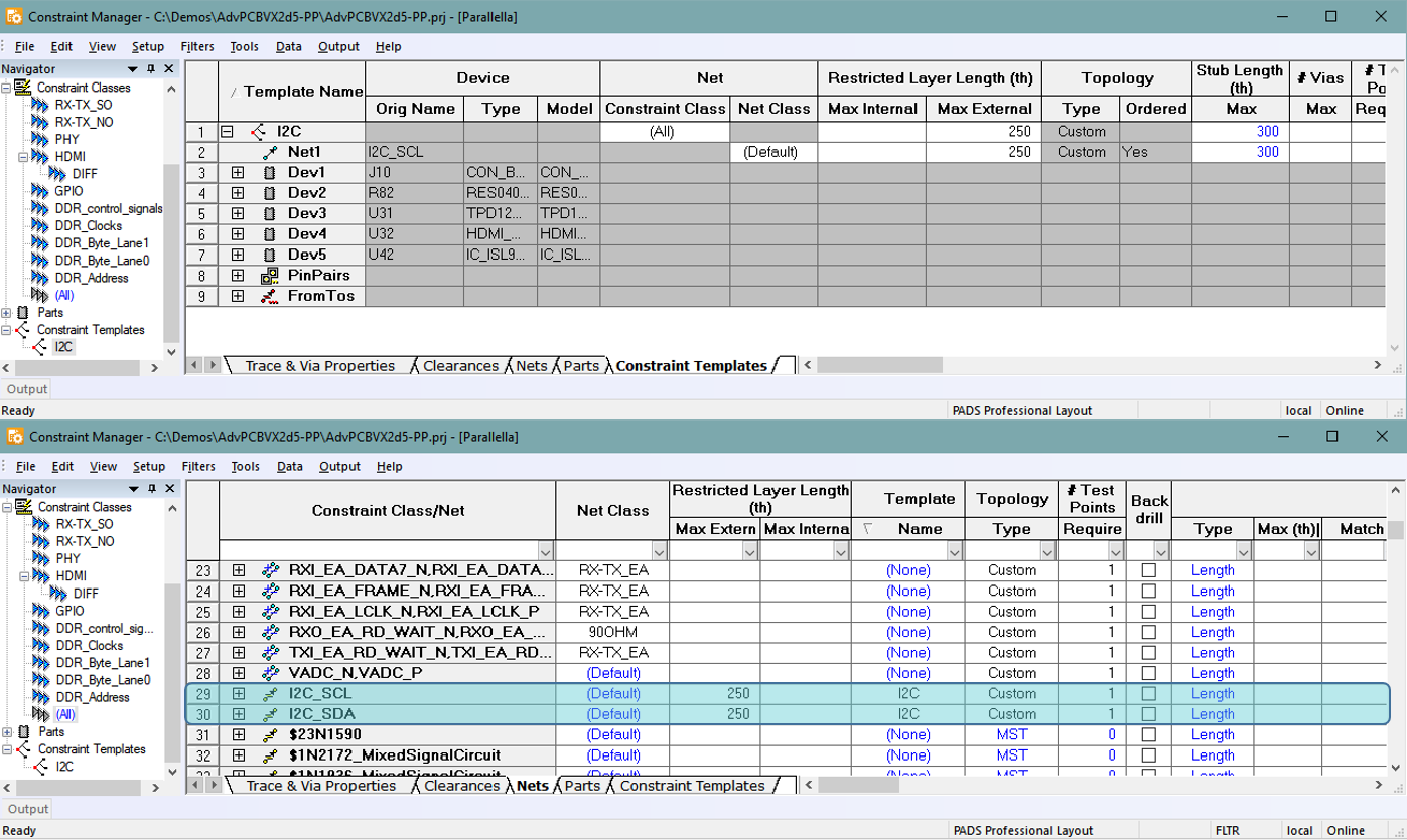
Another rule reuse option we have on the electrical rule side is Constraint Templates. These allow us to take a constraint definition for a net or diff pair with any of the following rules defined: net class association, topology definition including virtual pins, stub length, max vias, length, test point count, restricted layer length, formulas, and special differential pair rules. These can be saved to a constraint template that can be assigned to objects requiring the same electrical rules (Figure 8). The reuse part comes from, when we adjust one or several of the parameters, all nets or diff pairs assigned that template name will take on those changes. So, instead of having to manage the process of modifying all these individually we can now do it in one location. Lastly, Constraint Templates allow us to share design rules from one design to another via export and import.
Whether your experienced or seasoned board designer we should all be using some degree of automation for routing to dramatically reduce the most time consuming phase of a board design. During our next blog installment we’ll be covering routing and trace length matching using automation included with PADS Professional.


