Optimizing FPGA/PCB co-design: Best practices and industry insights
Previously on episode 20 of the Printed Circuit Podcast, host Steph Chavez explored the intricacies of FPGA (field-programmable gate array) and PCB (printed circuit board) co-design, which is an essential yet often challenging aspect of modern electronics. To discuss this topic, Chavez was joined by Gary Lameris, Technical Marketing Engineer at Siemens since 2008, to examine the challenges, best practices, and innovative solutions that shapes FPGA/ PCB co-design as we see today.
Challenges in FPGA/PCB co-design
“The printed circuit board engineer and the part librarians have to design their parts. So, by designing the parts specifically toward the FPGA design engineers specifications, they may be over straining in their system [which can] cause difficulties in routing, optimization, and performance of the printed circuit board,” said Lameris, emphasizing how FPGA design shouldn’t only be handled by the PCB engineer. –
Chavez highlighted the importance of “getting it right from the beginning” and collaboration to avoid problems in the FPGA design process. Another critical obstacle for design teams is not selecting the FPGA devices early, which leads to last-minute changes that disrupts the PCB layout and production timelines.
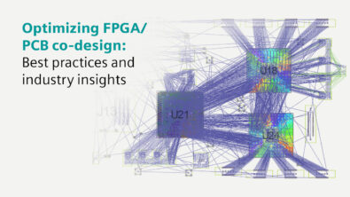
“Using this co-design functionality—especially with Xpedition—the grouping signals can be created easily to manage the complexity of high pin-count parts, especially when we think about the different sizes and how they’re becoming more and more dense and these FPGAs,” said Chavez.
Solutions to design challenges
It is crucial to ensure that FPGA and PCB engineers align on component selection and routing requirements ahead of time. Xpedition plays an important role in this integration, enabling optimized FPGA/PCB co-design. By using grouping signals and automated pin assignments, engineers can reduce design complexity and streamline PCB layout.
“With a product called IO optimizer, FPGA wizard. So, we have more than 18,000 models of FPGAs that we can read and then make custom symbols and match to a cell footprint that you need to actually place on your printed circuit board,” said Lameris., highlighting the reduction of human error and enabling of faster iteration cycles.
One of the biggest concerns in adopting FPGA/PCB co-design methodologies is the perceived time and effort required to implement these processes, but both Chavez and Lameris emphasized the increase in efficiency and cost savings for pin assignments and routing optimizations. “It’s been shown to reduce the numbers of layers a PCB has; it’s been shown to reduce your propagation delay; it’s been visibly shown to improve your routing,” Lameris explained. “The advantage of having a model built and the FPGA optimizer is that we can move these components around on the board, make design decisions on the fly, and reoptimize.”
Roadblocks to implement FPGA/PCB co-design
Many development teams and engineers often consider the process too complicated to incorporate a new system for FPGA/PCB co-design. However, it can end up saving multiple days and an increased sense of efficiency within the workflow.
“Where we moved the FPGA just a little bit, we rotated it; we changed where the memory banks were. All sorts of design decisions happened, and because we spent that time upfront learning how to create the initial model, all we had to do was spend minutes to re-optimize the design on the board,” said Lameris.
The reluctance to change was especially evident during supply chain disruptions post-COVID-19, when component shortages forced engineers to reconsider their designs due to the 52 weeks lead time of certain parts of a design.
“You have to be bold and show them the design efficiencies that can actually occur through automation,” Lameris emphasized.
Adopting model-based design approaches and automation of tools is vital to allow engineers to quickly adapt, reroute circuits, and optimize layouts without extensive manual redesigns.
”It is this seamless collaboration that you have between FPGA and PCB disciplines, to allow this co-design integration to really positively impact the results of the full design cycle,” said Chavez.
Conclusions
The integration of FPGA/PCB co-design has become an important factor in achieving optimized performance, efficiency, and manufacturability. Through early collaboration, automation, and using tools such as Xpedition and the FPGA wizard, engineering teams can streamline workflows, reduce costly iterations, and enhanced design accuracy.
Adaptability is crucial for success in the evolving electronics industry. Engineers and development teams must embrace automation and model-based design systems to stay competitive. By prioritizing FPGA/PCB integration, companies can future proof their design processes, reduce production risks, and drive novel innovation.
For more information on FPGA/PCB co-design, visit our website or watch this video.


Comments
Leave a Reply
You must be logged in to post a comment.
Read also: Visa status