Six challenges that make flex circuits more difficult to manufacture
Understanding the bend
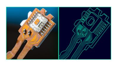
Flexible circuits, sometimes referred to as flexible Printed Circuit Boards (PCBs), are increasingly prevalent in compact formfactors such as wearable electronics, and mobile devices. Their designs require specialized manufacturing approaches distinct from rigid (PCBs). While early Electronic Design Automation (EDA) tools traditionally focused on rigid PCB designs, flexible circuits have been increasingly leveraged, as they provide improved reliability and reduced costs by replacing bulky connectors traditionally used with PCBs. Despite these improvements in manufacturing and design optimization, flex and rigid-flex designs remain expensive to produce.
In contrast to EDA progress in layout and routing, flexible manufacturing details like coverlays, solder masks, and stiffeners are often inconsistently communicated between designers and manufacturer partners, resulting in verification and production challenges. A robust Design for Manufacturing (DFM) solution for both flex and rigid flex circuits must incorporate a digital twin that accurately maps all relevant layers and materials, enabling automated verification and reliable fabrication for flex and rigid-flex circuits.
EDA solutions have been full of work-arounds when communicating the additional manufacturing requirements for these designs. EDA solutions rely on assigning user layers to communicate flex portions, and in this way, they also target critical flexible manufacturing processes areas such as the shape and placement of coverlays, LPI regions, metal shielding, adhesive, and stiffeners, to name a few.
A Manufacturing Driven Design (MDD) workflow targets the manufacturing verification of flex and rigid-flexible PCBs needs to be comprehensive to create a digital twin that not only prioritizes traditional rigid material, but can also create the relationship necessary to support flex and rigid-flex boards throughout the design process. The solution requires the ability to understand the relationship between coverlay, LPI, and dry film solder mask and copper layers, and communicate it in an effective and timely manner. Only once this manufacturing knowledge is delivering to the right person at the right time will a truly comprehensive flex and rigid flex digital twin be possible. Only once a comprehensive digital twin is at hand can a completely automated fabrication and assembly verification of flex circuits be effectively applied.
The flexible area of a board gives rise to manufacturing challenges that, if not managed well will negatively impact the reliability of the product over time. As such, there are several specific challenges to keep in mind when designing and verifying flexible circuits. The following are some potential situations to avoid when designing these regions.
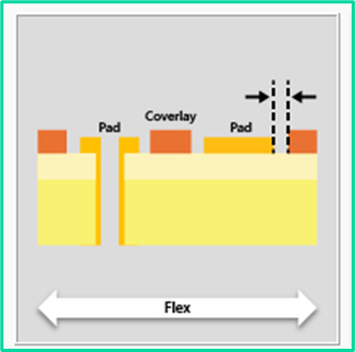
1. Non-solder mask (NSMD)/solder mask defined (SMD) pads
Within the flex portion of the PCB, the position of a copper pad relative to the bend area can have essentially two configurations; it can be a Non-Solder Mask Defined (NSMD) pad, or a Solder Mask Defined (SMD) pad. A NSMD pad is one where the edge of the coverlay, or possibly Liquid Photo-Imagable (LPI) solder mask, is positioned away from the pad edge, exposing the entire area of the pad, or a Solder Mask Defined (SMD) pad, which has the coverlay or LPI intrudes over the pad edge partially cover the copper pad reducing the size of expose area of the pad.
Having the edge of the pad partially covered provided extra bonding strength for the copper to the laminate material beneath and provides improved mechanical strength in the case of the pad having routed connections. The coverlay or LPI distance away from the copper pad edge or the amount of overlap on to the copper pad edge varies based whether the pad is drilled or not. This results in 4 possible DFM rule configurations for required overlap or necessary clearance for these areas:
Flex – minimum coverlay overlap for mask defined drilled pad
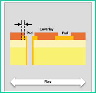
In rigid-flex and flex designs, which are prone to bending and flexing, using mask defining pads can be beneficial. The coverlay defines the pad boundaries for soldering, reduces the risk of solder bridging, and provides additional mechanical bonding strength to the copper pad on the PCB. Ensuring sufficient coverage of the coverlay on top of the pad is crucial to prevent the pad from lifting and to accommodate registration issues. The constraint measures the distance between the covered edge of a drilled copper pad to the coverlay opening in the flex region of the board.
Flex – minimum coverlay clearance for non-mask defined drilled pad
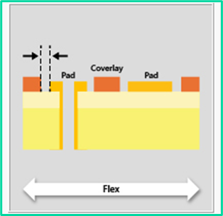
In rigid-flex and flex designs, non-solder mask defined (NSMD) pads allow the flexibility of pad shape and size to accommodate custom designs and assist in creating robust solder joints. It is important to ensure a sufficient gap between the pad edge and the solder mask edge to allow the solder to flow down to the sides. The constraint measures the distance between the edge of a drilled copper pad to the coverlay opening in the flex region of the board.
Flex – minimum coverlay overlap for mask defined undrilled pad
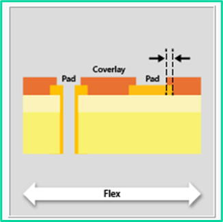
In rigid-flex and flex designs, which are prone to bending and flexing, using mask-defined pads can be beneficial. The coverlay defines the pad boundaries for soldering, reduces the risk of solder bridging, and provides additional mechanical bonding strength to the copper pad on the PCB. Ensuring sufficient coverage of the coverlay on top of the pad is crucial to prevent the pad from lifting and to accommodate registration issues. The constraint measures the distance between the covered edge of an undrilled copper pad to the coverlay opening in the flex region of the board.
Flex – minimum coverlay clearance for non-mask defined undrilled pad
In rigid-flex designs, non-solder mask defined (NSMD) pads allow the flexibility of pad shape and size to accommodate custom designs and assist in creating robust solder joints. It is important to ensure a sufficient gap between the pad edge and the solder mask edge to allow the solder to flow down to the sides. The constraint measures the distance between the edge of an undrilled copper pad to the coverlay opening in the flex region on the board.
The test conditions must consider the placement method, either by hand or photo imaging.
To properly covey this information to an automated DFM solution, the relationship between the user defined layers representing the coverlay and LPI to the associated copper layer needs to be established. The digital twin needs to be able to establish and carry forward that these user layers are associated with the manufacturing process of a select copper layer within the PCB stack up.
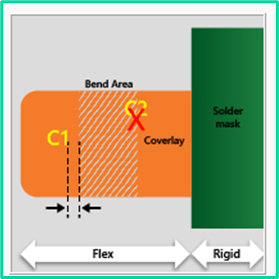
2. Coverlay transitioning into LPI solder mask
The placement of coverlay material is a manual process and is less accurate compared to Liquid Photo-Imagable solder mask, which is applied and then cured into place using UV light. The openings in the coverlay are created by a physical punch, or using a laser. Both of these methods provide positionings which are less accurate than the LPI process itself. In addition, LPI opening can be customized shapes and sizes without changing the tooling required to create the coverlay. This typically occurs when finer pitch components are on a flexible portion of the design.
To support this transition the LPI covered region is larger than the opening in the coverlay. Doing so will ensure that the LPI is applied over the edge of the coverlay, removing any air gap between the two edges, which would lead to the existence of unintended exposed copper.
Flex – minimum coverlay and LPI overlap
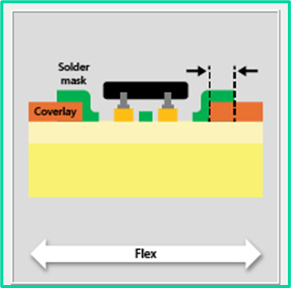
In rigid-flex and flex designs, the LPI solder mask must extend sufficiently over the coverlay edges in the flexible region to ensure proper protection against moisture, dust, and mechanical stress.
With the coverlay and LPI solder mask referencing the same copper layer within the digital twin, the automated DFM verification process can automatically ensure that the amount of overlap is suitable for manufacturing.
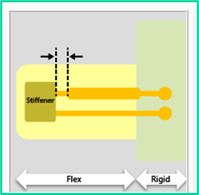
3. Stiffener positioning relative to a coverlay
A flex design’s obvious benefits also presents one of its biggest challenges. During automated component placement, or connecting the flex circuit to another board or cable during box build, the very flexibility of the board itself works against the necessary final construction. Sometimes, you just really just want to be working with a rigid surface.
To create this rigid surface, stiffeners are placed on the opposite side of the board, creating a support area where downward pressure can be applied while not damaging the flexible materials. To create this surface, a non-conductive coverlay is placed between the copper outer layer and the stiffener. This is very important when the stiffener is made from metallic materials.
In the case of connectors, the stiffener provides improved reliability because without a stiffener connector misalignment, damage solder joint, cracked copper, or mechanical fatigue would likely occur. As a general need, stiffeners also provide a safe rigid region to manually handle flexible areas for inspection and testing.
To ensure that the component or connection is mechanically supported, there must be an adequate distance from the edge of the copper pad to the inner edge of the stiffener material on the opposite side of the design. The distance is largely required because the stiffener is manually placed, and the accuracy is always in question. To ensure a stable copper surface is present, the copper edge when measured from the opposite side must be a suitable distance from the inner edge of the stiffener.
Flex – insufficient stiffener support to component SMD toeprint
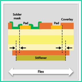
In rigid-flex designs, providing adequate stiffener support for components on the opposite side is essential for mechanical stability. This support allows the flexible portion of the PCB to bend without concentrating stress at the interface of the copper and laminate materials, thereby preventing potential damage to the copper pads. The constraint measures the distance between the edge of the component’s exposed SMD pad and the edge of the stiffener located on the opposite side.
Like the requirement for the placement of a stiffener, the edge of the copper pad must remain a required distance from the inner edge of the coverlay placed on the opposite side of the design. In this case the manufacturing outcoming to avoid are the pealing or delamination of the coverlay, or the cracking of the adhesive under the coverlay resulting from the position of the more rigid copper relative to the coverlay edge which asserts additional stress during flexing or thermal cycling.
Flex – insufficient opposite-side coverlay coverage for toeprint
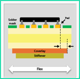
In rigid-flex and flex designs, it is essential to maintain consistent material beneath a component in the flexible section. To ensure this, the component’s copper pads must be positioned at a sufficient distance from the coverlay’s outer edge on the opposite side.
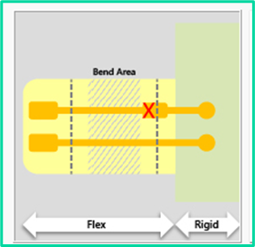
4. Copper changing width while approaching stiffener or bend area
A copper route, or line changing width while approaching a stiffener or bend area is to be avoided. Such a condition acts as a stress riser at the point of change during the flexing of the design. The stress can result in thinner sections of the base material cracking or can lead to delamination. Early detection and prevention will ensure that copper strength and material stability is prioritized while performing layout.
Flex – line changes width close to stiffener edge
In rigid-flex and flex designs, copper traces inside the flexible portion are subjected to compression and tension. A change in the copper trace width close to stiffeners can intensify this effect, potentially causing premature failure of the flexible material due to excessive stress.
Flex – line changes width outside bend area
In rigid-flex and fex designs, copper traces inside the flexible portion are subjected to compression and tension. A change in the copper trace width close to the bend area can create stress points susceptible to cracking and failure during bending. Consistent trace width helps distribute mechanical stress evenly. Changes in trace width inside the bend area are reported to the constraint Flex – line changes width in bend area.
5. Copper changing direction while approaching a bend area
Like the previous condition, a copper route or line changing direction while approaching a bend area should be avoided. Not doing so could result in copper fatigue, cracking and even board delamination. Lines running non-parallel to the bend axis will also reduce the flexibility of the board and require additional force to bend, eventually leading to these negative side-effects. The reliability of a board containing flexible regions is often determined by the accumulation of tradeoffs more than within most rigid board designs.
Flex – Line changes direction outside bend area
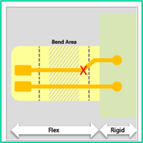
In rigid-flex and flex design, copper traces within the bent flexible portion are subjected to compression and tension. A change in copper trace direction near the bend area can create stress points susceptible to cracking and failure during bending. The constraint reports any change in line direction greater than the specified angle value inside the extended boundaries defined outside the bend area.
6. Silkscreen is too close to bend areas
The simple inks use to mark and identify components for reference and repairs are referred to as silkscreen. The traditional application method is really no different from applying an image to a t-shirt. Regions where ink is to be applied are removed from a sheet of material creating a stencil, the stencil is accurately placed on the outer layer of the design and ink is then applied through the holes within the stencil. A more modern approach is to print ink directly on to the outer layer of the design akin to creating a printed page using an ink jet printer.
When silkscreen is used within a flexible portion of a board, the outer layer the ink is being applied to must be rationalized. Once rationalized, the placement of the ink relative to the bend areas needs to be further scrutinized. Ink does not lend well to bending without cracking and separating from the board creating a mess within the environment where the board is placed. As a result, ensuring silkscreen keeps a distance from a bend area is critical to reliable use of a flexible board.
Flex – silk screen close to bend area
In rigid-flex and flex designs, it is important to avoid placing silk near or within the bend area to prevent cracking or flaking of the silk screen material due to flex stress concentration.
Valor NPI: Engaging with flexible design needs
Valor NPI is the leading flex and rigid-flex DFM verification solution providing designers peace of mind with every design release. Valor NPI reliance on the ever-improving ODB++ format combine to create the first solution to deliver a comprehensive digital twin built with a Manufacturing Driven Design (MDD) mindset, supporting both the rigid and flex portions of a board.
Valor NPI utilizes the wealth of flex knowledge within ODB++ to automate the application of verification requirements. Starting off where EDA solutions stopped, ODB++ contains flexible material layer details such as coverlay, LPI, metal shielding, metallic stiffener, FR4 stiffener, and much more. Each material layer is then referenced to the board layer each as an indication of the manufacturing process. This layer-to-layer connection enables a completely automated verification process as the digital twin carries forward the intelligence necessary.
Valor NPI’s has recently introduced these six new verification checks within the latest release available to customers to download off of Siemens’ Support Center. These checks, combined with the existing robust flex and rigid-flex DFM checks within Valor NPI copper and laminated materials remain intact during active bending.
We encourage you to download and test drive these checks with a completely free trial of Valor NPI.