The importance of design for manufacturability in the PCB design process
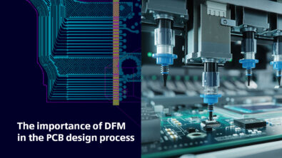
When it comes to designing and producing electronics, success hinges not merely on the excellence of your design, but also on how effectively and efficiently that design can be brought to life. That’s where the concept of design for manufacturability (DFM) comes into play. DFM is the process of designing for ease of manufacturing, and its importance cannot be overstated. Implementing DFM principles from the get-go in your PCB design process can streamline production, mitigate errors, and ultimately save substantial time and money.
So, you know design for manufacturability is important but how can you best incorporate it into your PCB design process? First, you can consider IPC guidelines and adhere to them as you design. Second, you can collaborate with your cross functional team throughout development to include your external stake holders (Fab and Assembly). Third, you can try to shift the DFM analysis left to discover issues prior to sending out for fabrication.
Adhering to IPC guidelines
Accuracy and attention to detail are important in the PCB design process. A small misstep in the design stage can lead to costly delays and quality issues downstream during the manufacturing stage.
Often, we might overlook the importance of double-checking and validating our work. Just as we might hastily send an email without re-reading it, the same can happen in PCB design. Documentation errors, outdated drill charts, or misplaced impedance lines can lead to significant delays in a process where time is of the essence. An astounding 70% of jobs could be on hold due to incorrect documentation, unmanufacturable design data, or unfinished designs. This is especially true in the military sector, where traceability and reliability are non-negotiable.
So, what’s the solution? The answer lies in the industry’s best practices and standards, particularly the IPC-2221, IPC-2222 for rigid boards, IPC-2223 for rigid-flex and flex designs, IPC-2226 for High Density Interconnect (HDI) printed boards, and the new IPC-2228 standard for High Frequency (RF/Microwave) printed boards. These design guidelines cover crucial aspects like pad sizes, drill minimum spacing, and other features. At a minimum, these should be considered and implemented when designing the board.
Let’s consider a real-life example. A PCB, initially yielding a 25% success rate, was redesigned in adherence to IPC rules, increasing the yield to a stunning 88%. The redesign didn’t involve changing the components, but rather followed the IPC guidelines as required. Taking the time to familiarize yourself with the IPC standards, applying these rules to the design process, and collaborating with your external suppliers significantly improves the final product’s success rate.
IPC guidelines provide an excellent roadmap for designing efficient and reliable PCBs. By studying and applying these rules, we can avoid unnecessary delays and increase the yield, ensuring high quality and reliability for our clients.
Open discussions can streamline design and production
During any PCB design project, it’s essential to know when to reach out to your production team for validation. In a conversation I had with Gerry Partida of Summit Interconnect he shared how this approach was clearly demonstrated.
A client called him with an interesting design proposal – they wanted to use a dielectric that’s less than the standard three and a half. This presented a challenge, but it was certainly feasible with clear communication and a sound understanding of the design’s objectives. It was clear that the client was struggling to balance the need for low dielectric with the required power and ground layers. After some discussion, they managed to find a solution that satisfied both the design and performance requirements.
Such open conversations are immensely useful in troubleshooting potential issues. For instance, the topic of internal blind or buried vias came up in this same discussion. The client was unsure about the possibilities and ramifications of stopping on a plane layer, rather than on an impedance layer with signals. Upon explaining the benefits – better and consistent yields, improved performance – the client was able to make an informed decision that eventually improved the design.
One of the most complex designs Gerry ever encountered involved six microvias deep. The initial design proposed stacking them all the way through, which was destined to fail. However, after extensive discussions and multiple design iterations, they were able to eliminate riskier layers, enhance yields, and build three different part numbers in four weeks.
Open collaboration between design and manufacturing/production can lead to successful outcomes, even with complex demands. The essence of such collaborations is open-mindedness and the willingness to challenge and negotiate design norms, ensuring that practicality and performance go hand in hand.
Considering design for manufacturability earlier in the design process
We must acknowledge that a design may not always be perfect in its first iteration. This understanding sets the foundation for a proactive approach towards identifying room for improvement and being ready to start over on certain parts of the design.
The design for manufacturability process traditionally involves the designer asking the manufacturing expert to review a design at the end of the process. The manufacturing expert then lists everything that’s wrong, and the designer has to then go back and change the design to remedy any issues that were discovered. The real value of the design for manufacturability process is in the reception and incorporation of feedback.
Incorporating a DFM analysis into your design process, instead of waiting until the design is complete is highly recommended and considered today’s industry best practice. The implementation of an industry-standard DFM tool like Valor NPI (which can be integrated right into Xpedition, so you don’t even leave your design environment) can enhance the efficiency of PCB design/manufacturing. Valor NPI ensures the feasibility of manufacturing, and its suite of process tools aids in generating complete manufacturing data. These manufacturing solutions aim for an optimized shop floor and successful ‘first-time-right’ electronics production.
Explore additional resources on implementing DFM in the PCB design flow
To learn more about design for manufacturability in the PCB design process you can also check out these additional resources: