PCB design best practices: power integrity analysis
What is power integrity analysis?
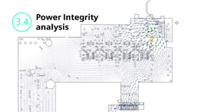
PCB power integrity analysis is the study of a PCB’s Power Delivery Network (PDN), which consists of the VRM, power planes/areas, decoupling capacitors and any other devices in the power supply path. It’s tempting to think of power integrity (PI) as simply ensuring that adequate power is delivered to the active components on the board, but a PDN really serves two different (but related) purposes:
- It delivers the appropriate voltage and current to powered components, meeting steady-state and surge current demands at appropriate frequencies.
- It provides a clean, continuous return path for high-speed nets, ensuring that signals travel from driver to receiver minimal disruptions and coupling. A poorly-designed PDN can result in interference between signals due to return path sharing.
Power integrity analysis normally occurs in three stages – the first two deal with component power delivery, while the third stage deals with interactions between high-speed signals and the PDN:
- DC analysis (also called DC Drop analysis) considers voltage drop and current flow within the system at maximum steady-state load. Power planes have finite resistance (small, but measurable). As IC voltages drop and speeds increase, the current demanded by ICs skyrockets – and the sheet resistance of power planes comes into play. It’s critical to manage the IR drop associated with that resistance by dropping the plane resistance, compensating for the drop (using a VRM with sense lines), or both.
- AC analysis (also called Decoupling Analysis) considers how the power delivered to ICs responses to fast changes in the demand for power, caused by switching events in the device core and I/O pins. The VRM is electrically too far away from the ICs to respond to these events, so decoupling capacitors act as local charge reservoirs to provide short-term power, albeit for a sharply limited time. The capacitor value, package style, fanout and distance from the IC determine the frequencies at which it will be an effective source of power.
- Power-aware analysis is signal-integrity analysis that considers interactions between the PDN and high-speed signals. This can be the result of Simultaneous Switching Noise (SSN) that occurs when multiple device outputs switch together, temporarily depleting charge at the IC’s driver power rail, or it can be the result of return path discontinuities. Return path discontinuities occur when a signal changes layers, such that return current flowing on the input signal reference layer has to find a path to the reference layer associated with the output signal.
Power integrity analysis is classically associated with DC and AC analysis; we include Power-Aware analysis in this discussion (even though it involves SI simulation techniques) because the electromagnetic modeling needed to create the interconnect model overlaps with the extraction and modeling techniques used for AC analysis.
How does someone know they need power integrity analysis?
The need for structured power integrity analysis is driven by the design – small, moderate-performance designs can probably get by with rules of thumb, while larger, high-performance, high-power-designs require formal analysis, because the operating margins are small. There’s no obvious “line in the sand” that determines which designs require analysis and which don’t – the adoption of analysis tools is often driven by a design failure.
What’s not working today?
The previous statement is an obvious problem – companies typically don’t pick up analysis tools until they have a design that fails in the lab. Ideally, structured analysis would get implemented before designs got to that point. That said – deploying analysis tools takes time, expertise and money – so there’s a natural inclination to put off until tomorrow issues that aren’t a problem today. As the old engineering maxim goes, “If it ain’t broke, don’t fix it”.
The challenge is that by the time a design fails in the lab, it quickly becomes a crisis. If the PDN was sufficiently under-designed, there may be no “quick fix” – a significant or complete re-design may be required.
What are the roadblocks?
One of the big challenges to board-level signal integrity is understanding what the design-specific performance requirements are in the first place. Processor clocks are in the 100+ MHz to multiple GHz range. The board-level PDN doesn’t need to provide power at those frequencies, because the IC package limits the frequencies than can be delivered from the board. Remember – the PDN provides IC power and a return path for high-speed signals. Most I/O signals are ground-referenced and those I/O signals do have to perform at high-frequencies. As a result, IC packages typically have many more ground than power pins, to provide those high-speed signal return paths. The (relatively fewer) power pins will have a higher loop inductance and need to carry much more current. That means the package has a natural power cutoff somewhere between 20 – 150MHz. The PCB could be designed to provide stable power to higher frequencies, but it won’t matter – because it wouldn’t make it through the package – any performance at frequencies higher than the package cutoff is a waste of time and money.
It’s not uncommon for the PCB power impedance requirement to be in the 50-100 milliohm range, from DC to 100MHz. Meeting a 75 millohm target at 100MHz is a lot harder than meeting the same target at 50MHz, so it’s important to get a good handle on what the package cutoff frequency is.
That said, establishing DC current requirements, surge current requirements and package cutoff frequencies can be difficult. Device manufacturers may not publish this data with enough detail, forcing designers to rely on estimates and rules of thumb that can drive up board manufacturing costs.
Another challenge is the time, effort and expertise needed to adopt power integrity analysis tools in the first place. Fortunately, the principles, models and analysis involved are simpler than their SI counterparts – making it more likely that a hardware engineer can perform this analysis themselves, without requiring a dedicated specialist.
Best practices: power integrity analysis
Power integrity is a foundational board design process – starting early and getting a plan in place greatly increases the chances for success. Early in the layout process, the board outline should be defined and critical components placed. Power planes and areas should then be added, which allows DC analysis to proceed. Analysis and design should proceed iteratively until a workable DC power delivery plan is in place; everything else builds on that.
Next, AC analysis should be run for the major components, placing and refining the decoupling arrangement until the AC power requirements are met. Signal Integrity analysis assumes the components have adequate core power – if that goal isn’t achieved, good signal quality won’t matter.
Establishing target impedances for AC analysis is difficult, because the data needed to establish package cutoff frequencies may be unavailable. Designers have to sort between hard data, estimates/rules of thumb and historical target values when determining a device’s impedance requirements.
Once decoupling capacitors have been placed, automated optimization can help improve the design. A good optimizer will use several different strategies for how the decoupling network achieves its goals, giving the designer a set of alternative implementations (and associated performance data) to pick from.
Once the PDN has taken shape, high-speed routing can begin. As with PI, starting early and putting a plan in place is key. If there are any doubts about the signal’s return path, then the combined signal/return path should be modeled and run with SI simulation. SSN isn’t typically an issue with SerDes channels, but it’s a significant issue with wide, single-ended interfaces like DDR. If the appropriate power-aware device models are available, power-aware SI simulation can model the combined effects of driver voltage droop and signal return path sharing, providing the most accurate estimate of design performance possible.


