PCB design best practices: schematic analysis
What is PCB schematic analysis?
PCB schematic analysis is the automated analysis of each net within a schematic prior to pre-layout simulation and layout.
What’s not working today?
When we’re talking product design, the basic sequence of operations is:
- System definition
- Schematic
- Schematic verification
- Pre-layout simulation to define routing constraints
- Layout
- Layout DRC
- Sign off simulation
- Design for manufacturability assessment
The most error prone and tedious aspect of this process is the schematic verification segment. It involves several folks scanning with a magnifying glass to determine whether logical conundrums have made their way into the end product. It’s the one area where regardless of preventative considerations, mistakes are inevitable. From missing pull-ups, capacitor derating failures, incorrect symbols, on and on, good luck trying to find them all in any kind of efficient manner.
Best practices: schematic analysis
A best practice for schematic analysis exists, and it’s rather delightful. Don’t get too excited, it won’t design your schematic for you. What it does do is provide tool-driven sign off while eliminating the need for time sinking manual design reviews.
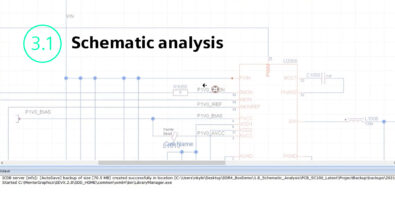
Xpedition schematic analysis enables full inspection of all nets on a schematic using an extensive intelligent model component library. Schematic analysis saves design teams hundreds of hours of visual inspection and lab debug time by analyzing each net within a schematic. This analysis executes rapidly prior to your schematic freeze milestone, such that layout may commence with highest confidence of first-pass success.
How it works: schematic analysis
Xpedition schematic analysis doesn’t rely on your library like a native schematic checker would, we take the manufacturer part number of each component straight from your Bill of Materials and create models so the issues mentioned before, capacitor derating failures, incorrect symbols, missing pull ups on and on are identified without the need for time bleeding magnifying glass manual effort exertion. The end output is a neat graphical representation of critical, defect and warning situations from which you can cross probe directly into the schematic to resolve on the fly.
Schematic analysis is performed in parallel with design capture, with errors highlighted directly in the schematic. It can also be performed on electronic designs after they have been released into the market to improve the quality of the electronic design, to increase yield, and to decrease product returns.
To learn more watch this video or visit our schematic analysis webpage.
Sound too good to be true? Ship us a known problematic schematic that went through several iterations and see what happens or schedule a demo.