Routing automation

One of the most critical and time-consuming part of the PCB design cycle is interconnecting the design. Typically, this is accomplished by “stitching” the trace from one pin to another, but by incorporating routing automation, PCB layout time can be reduced by up to 80%.
PCB Design challenges
Designs continue to become more difficult regarding interconnect. More functionality is being packed onto smaller substrates and faster components result in more high-speed constraints that must be maintained. Because cost is always an issue adding layers may not be advisable. Engineers and designers really must have routing automation to get their job done!
Constraint definition
PADS Professional Premium delivers unique technology that combines ease-of-use with highly automated PCB routing functionality that results in accelerated time to completion. It starts with constraint definition. These include mechanical rules such as trace width, clearances, and even which layers the trace can or cannot be routed on, as well as electrical rules such as length or time-based rules.
Once constraints are entered in the spreadsheet-based constraint editor, interactive routing can begin, and you can have confidence that all constraints will be adhered to. During interactive routing, as the trace is be added, all clearances will be met as you move your cursor, and the trace and necessary bends are automatically added. Push and shove can be enabled, moving other traces out of the way of this new trace, always maintaining minimum clearances. If a differential pair is routed, once one net is selected, the other net of the “pair” is automatically selected. As it’s being routed, the pair is maintained, routed together while maintaining the specified gap between the two nets.
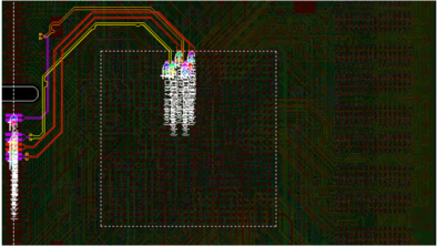
Sketch routing
PADS Professional Premium also delivers Sketch routing. With Sketch, the user selects multiple unconnected traces, such as a bus, and then “sketches” the path they would like the bus pattern to go. The next step is to select “route,” and the system will find the optimal path for these selected traces. Sketch routing delivers quality results and significantly reduces routing time, allowing you to move on to the next phase of the PCB design cycle.
Minimize design time by up to 80%
Interconnecting a design is an important and time-consuming step of the PCB design cycle. Including routing automation as part of your design process will ensure that all constraints are adhered to and can minimize the overall design time by up to 80%.
To learn more about routing automation with PADS Professional Premium, read our eBook.