Fundamentals of SI (Part 3) – Impedance
We’re finally on to the next logical step in our study of signal integrity – impedance. So what is impedance and why does it matter?
Impedance is a result of the physical properties that make up your PCB and the reason you care about this is because the impedance of your traces will have an impact on the signal quality. If you remember from Part 2 of this series on transmission lines, I talked about critical length. Well, one important aspect of transmission lines left out of that topic (on purpose) was that once t-lines are beyond the critical length, the impedance becomes important because it can cause reflections and distort signal quality. Matching impedance for driver, transmission line, and receiver becomes important to ensure you’ve got good signals at the receivers. Reflections are a topic in-and-of themselves, so I’ll reserve that for a future post, but below is what you need to know about transmission line impedance.
The basic formula for characteristic impedance is:

We can see that it’s made up of the capacitive and inductive properties of the trace. So what does this mean to a board designer? You can impact what the impedance of your traces are, largely based on your stackup design. Here are the main things in the stackup that we can use to control the impedance: dielectric thickness, dielectric constant, and trace width. The copper thickness can also play a part but it is less significant.
With dielectric thickness, we’re trying to determine how far away the trace should be placed from it’s reference layer(s). This is often ground for ideal situations but it could be a power layer as well.
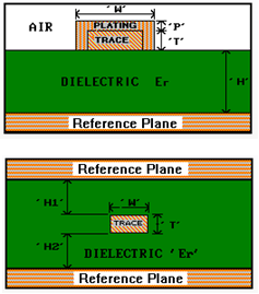
We also need to consider that the trace could be a microstrip (on the outer layer of the board) or a stripline (on an inner layer with references above and below the trace) structure. There are other types of structures such as dual stripline or buried microstrip but I just wanted to provide an example of 2 of the primary types of structures you’ll deal with. In both examples, when you decrease the dielectric thickness, you’ll decrease the impedance. Likewise, increasing thickness will increase impedance. Generally speaking, for the same dielectric thickness and trace width, you’ll have a higher impedance on a microstrip line than you will for a stripline because of the additional capacitance provided in the stripline structure.
The other important piece relative to the dielectric is the dielectric constant. Standard FR4 material in most PCBs will have a relative dielectric constant (commonly seen as Er or Dk – these symbols are interchangeable) on average of about 4.3 but if you choose a dielectric with a much lower Er, it will cause the impedance to increase. Similarly, if you were to increase the Er, it would cause the impedance to go down. The leaver you have to control the Er is the laminate you choose for the stackup design. If you want to see your options in more exotic materials, check out Isola or Rogers who are just two options of several in the laminate material industry.
The last factor that can play a major part in trace impedance is the trace width. If you increase the trace width, the impedance will go down. If you decrease the width, the impedance will go up.
So what makes all these properties behave the way they do? You can trace most of the changes down to how the capacitance is calculated. Looking at the equation for capacitance in a parallel plate, we can see there is dependency on dielectric constant, separation between the plates (d), as well as the area (A).
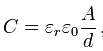
We can see that if the Er changes, that has a direct relationship on the capacitance. And going back to the characteristic impedance equation, it has an inverse relationship on impedance (e.g. Er goes up → impedance goes down). We can also see that as the separation between the two parallel plates increases, it has an inverse relationship on the capacitance, which means it has a direct relationship with the impedance (e.g. separation goes up → capacitance goes down → impedance goes up). And lastly, the area changes based on the trace width, so if the trace width goes up, capacitance goes up, which means the impedance goes down.
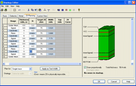
There are stackup planning tools in HyperLynx as well as Expedition which can simplify your life when it comes to impedance planning. It can be as simple as entering a target impedance for a layer given a certain stackup and HyperLynx will tell you the the trace width you need. Or you can enter a width and it will give you an impedance on any given layer.
I’ll leave you with some final thoughts on impedance control from a practical perspective. For most companies, if you design impedance controlled boards, your manufacturer is going to adjust whatever values you give them to hit the target impedances based on the materials they have on-hand. You may specify 6 mil width for traces and they may do 5.6 mils in production, but the end result that matters is that they are meeting your target impedance. One trick to give your manufacturer more ability to hit impedance goals is to specify slight differences in trace width for your targeted impedances, especially when it comes to differential impedance (I haven’t even touch on differential impedance here so I’ll save that for another post ). For instance, on Layer 4 of your stackup, you may have a 50 ohm target impedance which results in a 5 mil trace width for single ended traces, and a 100 ohm differential impedance with 5 mil traces on the same layer. For the single ended traces, just put 5.1 mils into your design and for the differential, make it 4.9 mils. That will allow them to target both impedances for you independent of each other without having to make compromises to either target impedance.
To learn more about impedance and stackup planning, check out Chapter 10 of the HyperLynx QuickTour.


