Fundamentals of SI (Part 2) – Transmission lines
Break out your calculators boys and girls because it’s math time (well….maybe you won’t need them after you get to the bottom of this post, but it’s fun to dust them off every now and then). The second part of this fundamentals series is going to talk about transmission lines and what exactly is a transmission line and how does it relate to a critical net (from Part 1)
Back in the good ole’ days, a transmission line use to carry your voice across the country – some may remember something called a “rotary telephone” and “landline“. The latter we had to make up in the recent decade because of those pesky cell phones. The point though, is that behavior across telephone lines is really not any different electrically than what is happening on your circuit board. If you ever made an international phone call before fiber-optic cable existed on the ocean floor, you can probably remember talking to some one, waiting a few seconds and then the other person would hear what you said, you wait a little bit more and they respond. It was slow and painful, but you knew that it took some time for your voice to travel halfway around the world. You didn’t experience that when you called down the street or the next state over though, right? Intuitively, you knew that it took some time for your voice to travel that far distance.
Now translate that to your circuit board. Because the distance between ICs on a PCB is relatively short (especially in comparison to a telephone line), people often don’t think about the time it takes for signals to travel on the PCB. But time is relative, and for something that is switching with edge rates that are below 1ns, that short distance between the ICs can seem like it’s a trip halfway around the world. The delay of that trip, know as the velocity of propagation, is fairly easy to calculate, especially on typical FR4 material.
Lets take a look at the math for the velocity of propagation:
Vp = c/√(μ*εr)
Here c is the speed of light, μ=1 since we have non-magnetic materials, and εr is the dielectric constant. Typically for FR4, the dielectric constant is ~4.2. There is some variability to that number, but I won’t get into that detail here. Going with that, we can see that Vp on a PCB is about equal to Vp=c/√4….1/2 the speed of light. That was easy math!
So we know that signals can travel about 6″ per 1ns from this quick and dirty math or invert that and you get 165 ps/inch – lets call this propagation delay the trace delay. These are important (and handy) numbers to remember, so you might want to jot them down somewhere.
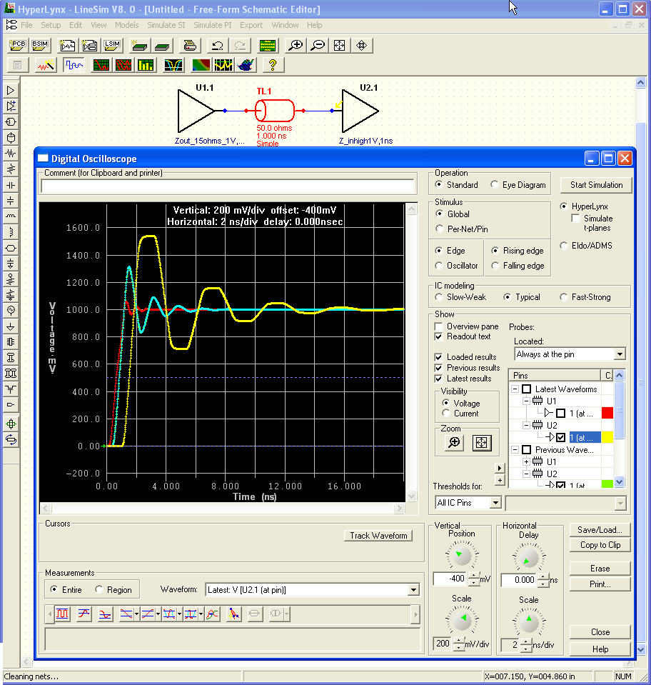
Those are cold hard facts about your PCBs electrical behavior as signals travel along traces, but now we get into the subjective part, which is critical length. Critical length compares that trace delay we just calculated to the edge rate of your signal to determine if we might have quality issues with that signal. Many times, you’ll see the rule of 1/3rd rise time to do this comparison. While this is a good starting point, it may not be good enough to meet your quality requirements. You may actually want to be more conservative and use a rule like 1/6th rise time to catch potential issues. Here’s a simple example below where I’ve got a 15 ohm driver with 1V swing and a 1ns edge rate. The receiver is a high impedance CMOS input, and the transmission is 50 ohms with varying delay of the rise time. You can see from the plot that we still have substantial 300mV of overshoot with a 1/3rd rise time rule and we may have missed this problem if we used that less conservative number.
Regardless which fraction of your edge rate you choose, it’s important to remember that the trace delay and the edge rate are closely tied to maintaining signal fidelity.
One thing I’ll point out here is that I never talked about the operating frequency. The most important thing you can take away from this post is that signal quality depends on edge rate, not operating frequency. Look for those fast switching edges in your design, not just the buses that you think are fast because they have a 400 MHz clock.
Now that we are warmed up a bit with regards to delay and edge rate, next time, I’ll dive into impedance next time to begin linking things together.
If you’d like to learn more about signal integrity and would like to check out how HyperLynx can help you identify problems like I’ve shown above, check out the new HyperLynx Signal Integrity Quick Tour. It’s a great resource to get up-to-speed on how to perform simulations for the most common signal integrity issues in your PCB design.


