Tackling compute complexity in ESD verification with Calibre

By Matthew Hogan, Product Management Director, Reliability Applications
Integrated circuit (IC) complexity is scaling at a pace that challenges every aspect of chip design, verification and manufacturing. As process nodes advance, devices become smaller and circuits more interconnected—especially with the shift to 2.5D and 3DIC structures—reliability engineers and ESD specialists face an ever-steeper mountain of verification tasks. In this environment, ensuring robust electrostatic discharge (ESD) protection becomes even more crucial—and computationally intense—than ever. The stakes are high: ESD failures can cripple a device at any stage, risking reputation and revenue.
This blog explores why compute complexity is rising in ESD verification, and how Calibre PERC and Calibre 3DPERC remain the dominant force in delivering signoff-quality verification for the world’s leading semiconductor companies.
Understanding ESD threats in modern semiconductor designs
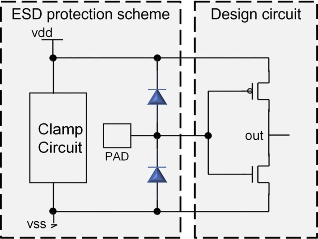
ESD is a fundamental reliability threat for ICs. It occurs when a sudden surge of electrical energy flows between charged objects, potentially causing metal to melt, junction breakdown, or oxide failure. Traditional chip layout techniques to protect against such events include use of fingered interdigitated devices, clamps, and other protection circuits that follow established design rules and best practices (Figure 1).
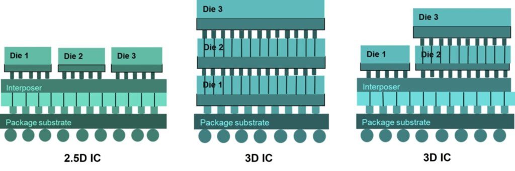
For decades, the number of external pins and their internal connections have permitted physical measurement in specially designed testers to validate that protections and their associated checks sufficed for single-die ICs. But today’s architectures have moved far beyond simple single die layouts. The industry is embracing 2.5D designs (multiple dies side-by-side on passive interposers) and 3D ICs (vertically stacked dies communicating through through-silicon vias). In these layouts, protection must account for new points of vulnerability: interfaces between dies, layers, and technology nodes—each with unique reliability and ESD rules. With recent innovations in hybrid bonding of these advanced architectures, physical verification of these interfaces becomes problematic. Pin counts and densities are exceeding the capabilities of physical test equipment. EDA tools must now be relied upon to fill this gap.
Why ESD verification got complicated
Compute complexity in ESD verification arises from several industry shifts and technical challenges:
- Multiple power domains and more devices: More domains increase the complexity of determining which potential ESD sources and sinks interact, what circuit constraints are needed and protection requirements for each of these domains.
- Interconnected topologies: Modern ICs feature thousands of external interconnected pins and ports. Exhaustively checking every possible discharge path is computationally demanding. When these connect to internal 3D IC structures with hybrid bonding, these paths rapidly grow into the millions. With many of these interfaces internal to the 3D IC structure, physical testing becomes problematic.
- Geometric and topological analysis: Checks combine geometric constraints (such as point-to-point resistance (P2P) and current density (CD)) and topological information (connectivity, correct protection device implementations and relationships between supply pads and devices).
- Scale and hierarchy: Hierarchical designs facilitate block re-use, but require verification at cell, macro and full-chip and assembly levels. As designs maturity migrates from early standalone cells/blocks through macro and complete assemblies, new combinations of possible ESD paths are introduced and must be verified.
- Technology diversity: 2.5D/3D ICs mix dies from multiple process nodes and foundries, each with their own ESD rules and constraints.
- Path-based checking: Interconnect robustness depends on P2Presistance and CD checks for each path—from pins to clamps, clamps to clamps, and pins to pins. Accurately measuring these requires precision layout extraction across all metal/via layers. Determining how to efficiently and accurately makes the necessary measurements from specific devices, cells, or only at the top cell level.
Just defining all these checks manually is a monumental task—and running a brute-force verification flow on large layouts or stacks simply isn’t practical without leveraging advances in automation and algorithmic efficiency.
Calibre: addressing compute complexity at every level
Siemens EDA has been at the forefront of this challenge, with Calibre as the dominant solution for physical and reliability verification. The Calibre PERC verification capabilities continue to evolve to tackle the significant compute complexity necessary for success, through several key approaches:
Efficient ESD device identification
ESD protection cells are usually well-identified in design databases but still need to undergo careful topological validation to ensure that appropriate protection devices are located where they need to be. With a bottom-up approach, validated macro blocks can be validated, enabling streamlined top-level connectivity checks and efficient path analysis.
Advanced P2P and CD verification for 2.5D and 3D ICs
Calibre PERC’s P2P and CD checks drive efficient interconnect verification across the most critical discharge routes. These critical paths are described in a rule deck, often from a foundry for each process node.
For advanced architectures, Calibre introduces the 3DPERC (die2die) methodology. This process automates ESD verification across die/interposer and assembly levels, integrating layout extraction, database creation, and stack-level rule analysis. The result is comprehensive assembly-level P2P/CD reporting that covers discharge paths of interest and reveals hidden vulnerabilities in even the most heterogeneous stacks and leverages an Innovator 3D IC or Calibre 3DStack assembly description of how each of these dies go together. Inputs include:
- Layouts for each die/interposer
- P2P/CD results database for each path in the design
- Assembly definitions and stack configuration
- ESD experiment and path descriptions for the 3DIC design
Once run on the entire assembly, Calibre 3DPERC provides results for efficient debug.
This process scales efficiently, rapidly simulating and analyzing all identified paths within the assembly and producing actionable results without overwhelming compute resources.
Context-aware ESD simulation for increased fidelity of protection margins
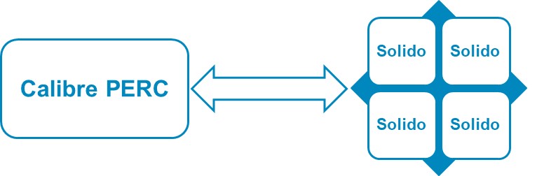
As layouts grow in size and design margins push against power, performance and area (PPA) targets, many design engineers seek to better understand design margins to avoid unnecessary overdesign. Typically, rule decks provided by the foundry or customer’s internal rules provide interconnect resistance constraints on ESD paths to encourage an ESD event to traverse through the designed ESD protection paths and avoid damage to sensitive logic circuits. These design rules are often conservative, catering for a broad range of mission profiles and design criteria. For ESD paths close to these interconnect resistance constraints, it is often desirable to seek greater fidelity of results in these specific design paths, Calibre PERC integrates context-aware ESD simulation capabilities into the design flow which greatly reduce the traditional SPICE simulation runtime of such circuits by providing a link to Siemens’ Solido Simulation Suite ( Figure 3) for use with ESD breakdown models, provided by either the foundry or customer’s own.
Based on the simulation waveform results, a determination can be made if these ESD paths require modification or are suitable, based on the increased fidelity of results that simulation on these marginal nets within the design provides (Figure 4)
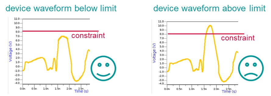
This combined solution enables full-chip ESD verification with increased fidelity—pinpointing paths at risk, simulating realistic breakdown scenarios, and quantifying ESD design margins.
Calibre’s customer impact and leadership
Industry leaders such as STMicroelectronics and Silicon Labs have chosen Calibre PERC for ESD verification. Watch how STMicroelectronics use in-design schematic checking to streamline their ESD design protection flows. Silicon Labs, who were a lunch partner for the context-aware ESD simulation technology when it was introduced at the Design Automation Conference (DAC) in 2024, describe their involvement with this technology at DAC 2024. These success stories highlight Calibre’s unique ability to deliver trusted results faster, even as chip architectures grow in complexity.
Conclusion: The path to reliable ESD protection
As IC complexity and 3DIC integration escalate, ESD verification isn’t just a technical challenge—it’s a computational race. The dominant role of Calibre in tackling this challenge underscores its leadership in signoff-quality reliability and physical verification. Whether you’re safeguarding a planar device or pioneering a stacked 3D IC design, Calibre’s scalable workflows help ensure your designs are ready.
To learn more or explore real-world customer outcomes, download our technical papers:
- Design optimal ESD protection using context-aware SPICE simulation
- Calibre 3DPERC: Your key to robust ESD solutions for 3D ICs
Doing more—faster, with Calibre—means you’re ready for the growing demands of tomorrow’s ICs.