Self-Aligned Double Patterning, Part Deux
By David Abercrombie, Mentor Graphics
Part 2 of a walk-through of the SADP process.
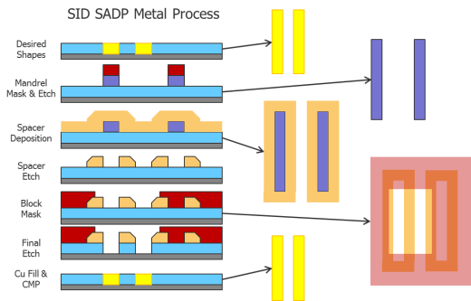
In my last article, I introduced you to the basic Self-Aligned Double-Patterning (SADP) process that is one of the potential candidate techniques for processing metal layers at 10 nm and below, but let’s have a quick recap. SADP uses a deposition and etch step process to create spacers surrounding a patterned shape (Figure 1). As you can see, there are two masking steps—the first mask is called the mandrel mask, and the second is called the block mask. These masks are quite different from the masks we are used to seeing in single-patterning or LELE double patterning processes.
Figure 1: SID SADP Metal Process.
Since spacer material is deposited on each side of the original shape, two shapes are created for every one shape originally defined, essentially pitch splitting the original lines (notice that the two mandrel mask shapes in Figure 1 produce four spacers at half the pitch). In the metal process application, the spacers define the gaps that will become dielectric material between the desired trenches that will be filled with copper to form the interconnect wires. Because these gaps between the wires will contain dielectric material, this form of SADP is called Spacer-is-Dielectric (SID).
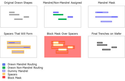
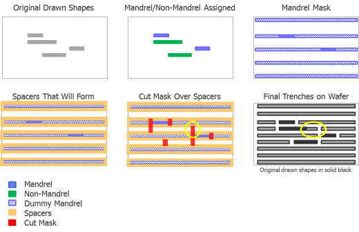
It is difficult for humans to readily visualize how these two masks produce the drawn shapes on the wafer. However, combined with the spacer deposition and etch process steps, they do, in fact, replicate the drawn shapes on the wafer (Figure 2).
Figure 2: SID SADP layer decomposition.
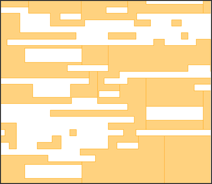
Looking at the two masks, the mandrel mask looks the most like the masks we are used to seeing and processing. It is essentially a bright-field mask with some lines on it. The block mask, however, is clearly a dark-field mask with holes in it. It is natural to think of this like a contact mask, but unlike a typical contact mask, the holes are not regular sizes. The example shown in Figure 2 is overly simplified, as all the original drawn shapes are unidirectional. Figure 3 shows an example of how a 2D layout can lead to much more complex block mask shapes.
Figure 3: Block mask when 2D shapes are present in the original drawn layout.
It turns out that trying to robustly image such a complex dark-field mask is very difficult. For this reason, it is likely that the layers for which this process is used will be very restricted, potentially to the point of only allowing unidirectional routing. However, even with a unidirectional layout, the block mask can still be quite complex in many cases.
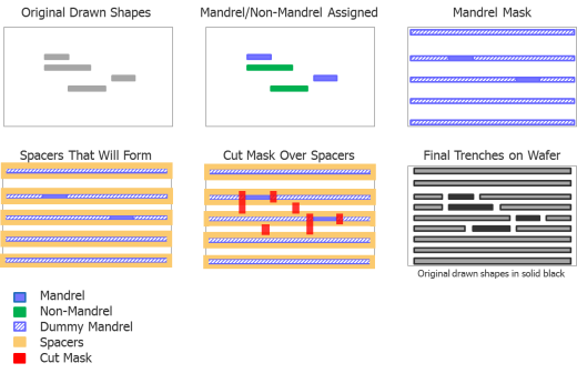
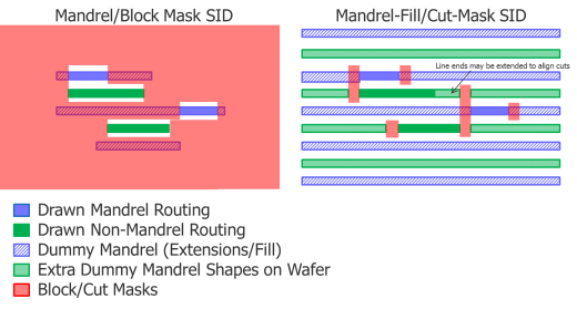
There is an alternative approach to SID SADP that may help with this issue. Figure 4 shows the same layout from figure 2, but using an alternate mandrel-fill/cut-mask approach. The initial coloring assignment of the drawn shapes to mandrel and non-mandrel is the same as the previous approach. However, the mandrel mask is different. The mandrel shapes are extended horizontally to the borders of the region being processed. In addition, complete dummy mandrel rows are added to fill the space vertically, a technique called mandrel fill. The end result is that the entire region now looks like a diffraction grating of parallel lines. As you might imagine, this image is very lithographically-friendly. When we get to the second mask, there is no longer a block mask, but a cut mask in its place. A cut mask contains simple rectangles that create cuts in the lines, which are also much more lithographically-friendly than a complex block mask. The end result on the wafer is a little different as well. You still get the originally desired drawn shapes (shown in black), but you get a grid of other lines (shown in grey) in addition. These lines are not electrically connected to anything, so the actual connectivity of the circuit is the same as the drawn layout.
Figure 4: Mandrel-Fill/Cut-Mask Approach to SID SADP.
This approach is much more robust from a manufacturing standpoint, but it does incur a little extra capacitance, due to all the dummy mandrel shapes around the drawn shapes at minimum distance. However, regular dummy fill requirements at these advanced nodes are usually at minimum distance anyway, so there is little difference from the capacitive impact standpoint.
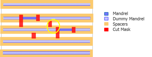
There are some key constraints on the router in this approach in terms of the spacing between cut mask shapes. Different cut mask shapes cannot be arbitrarily close to other cut mask shapes. For instance, the spacing of the highlighted cut mask shapes in Figure 5 may not be manufacturably robust.
Figure 5: Non-Manufacturable Cut Mask Spacing.
Such line-end to line-end spacings must be restricted in the router to avoid such problems. However, there is a “ sliding cut” variant on the technique shown in Figure 4, in which the cut mask shapes are shifted during decomposition to “fix” these issues [1] (Figure 6). To fix the spacing issue shown in Figure 5, the cut has been moved to the right to align with the cut shape below, which alleviates the spacing error. However, this ultimately changes the shapes on the wafer. As you can see in the highlighted wafer trenches, the original drawn shape (shown in black) has been extended, due to the moved cut shape. From a connectivity standpoint, nothing changes, as the via that will touch the end of the black shape will still land on that point, and the extended line does not create a new connection. The only significant difference is that there is extra metal hanging off this net, which adds additional capacitance to that net. Assuming these shifts are minimal, and the nets are relatively long with reasonable performance margin, this capacitance probably won’t cause any timing violations, but it must be evaluated to make sure.
Figure 6: Mandrel-Fill/Cut-Mask Sliding Cut Approach to SID SADP.
This sliding cut approach allows for a potential relaxation of the router constraint rules, but adds some complexity to the decomposition, and potentially the timing extraction and analysis. Figure 7 shows a side by side comparison of the traditional SID SADP and the mandrel-fill/cut-mask version of SID SADP for comparison.
Figure 7: Comparison of Traditional and Mandrel-Fill/Cut-Mask SID SADP.
It remains to be seen what type of approaches will be adopted by the various foundries and how these choices will affect the final design rules. Regardless, just trying to keep all these techniques and their variations straight in my head makes me feel like I am trying to pat my stomach and rub my head while riding a unicycle blindfolded on a tightrope. Challenging, for sure, unless maybe you work for Le Cirque.
In my next blog, I think it makes sense for us to spend a little time pondering the question about whether all this multi-patterning stuff is good for us or not.
Author
David Abercrombie is the Advanced Physical Verification Methodology Program Manager at Mentor Graphics. For the last few years, he has been driving development of EDA tools that can solve the issues in design to process interactions (DFM) that create ever-increasing yield problems. David received his BSEE from Clemson University, and his MSEE from North Carolina State University. He loves to play the guitar, explore the great outdoors, and watch a great science fiction show, but not all at the same time.
References
[1] Hongbo Zhang, Design-Technology Co-Optimization In Next Generation Lithograpy, Doctoral Thesis, University of Illinois at Urbana-Champaign, 2012
This article was originally published on www.seminengineering.com

