IC visualization: Supercharge debug of hidden parasitic threats with Calibre
By Omar Elabd
If you’ve ever watched your simulation pass with flying colors, only to see your silicon fail in the lab, you know the true frustration of invisible design issues. As chip manufacturing moves to cutting-edge nodes—7nm, 5nm and beyond—parasitic effects like resistance, capacitance and inductance are no longer minor footnotes. They’re major roadblocks to performance and reliability. And the most dangerous ones are often hidden where a netlist alone can’t reach.
Below, we’ll explore how advanced visualization techniques—like heat maps, layer-based analysis and physical-to-electrical mapping—help IC teams to spot, understand and fix these hidden enemies in their designs. Whether you’re a current Calibre xACT or Calibre xRC user looking to up your debug game, or investigating next-gen workflows, it’s time to move beyond educated guesswork and bring clarity to your silicon.
Hidden parasitics: the silent saboteurs of modern chips
Parasitic effects arise not from what you designed on the schematic, but from how the design gets laid out and fabricated. Routing, stacking and even proximity of metal layers creates unwanted resistance, capacitance and inductance in your chip. These parasitics grow exponentially as designs shrink and become more complex—especially for high-speed, high-density and 3D structures.
Why does this matter? At the 5nm node, parasitic delays can dominate your timing budget, accounting for over half of the total signal delay! That’s a dramatic shift from previous nodes, where parasitics contributed just a fraction. And the cost of missing these issues is high: industry analysis shows that parasitic-related silicon failures can set development teams back by weeks of debug per incident.
Traditional netlist and text-based reviews just don’t provide enough visibility. To break free from the “why won’t this work in the real chip?” trap, advanced visualization is essential.
Where netlists fall short
Let’s look at a few real-world scenarios where parasitic issues hide in plain sight:
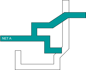
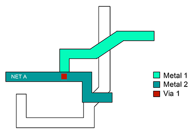
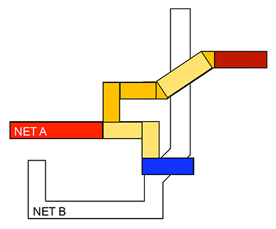
- High-speed signaling (PCIe, DDR, SerDes): A tiny mismatch in parasitic capacitance—sometimes as little as 5%—can cause crippling bit errors and link failures. The root cause may lurk somewhere between layers or along an overlooked route (figure 1).
- RF and high-frequency design: Circuits above 20 GHz are incredibly sensitive to inductive and capacitive effects. Minor layout changes can cause 30% or more degradation in signal fidelity.
- 3D architectures (FinFET, GAAFET): With stacked layers, parasitics don’t just multiply—they become harder to visualize and manage.
In every case, the challenge is the same: what’s not visible in your netlist can dominate silicon behavior.
Making parasitics visible: visualization that works
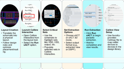
Modern EDA workflows—such as those enabled by the Siemens Calibre platform—now integrate multiple visualization and analysis tools, allowing teams to chase down these elusive design threats.
Turn raw data into insight with heat maps and layering
Imagine instantly spotting problem areas with a glance: heat maps use color to highlight hotspots for resistance, capacitance or inductance. With intuitive gradients, trouble areas leap off the screen—no more hunting through endless tables.
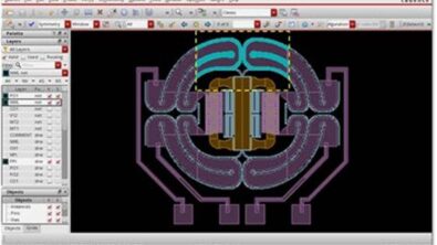
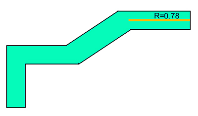
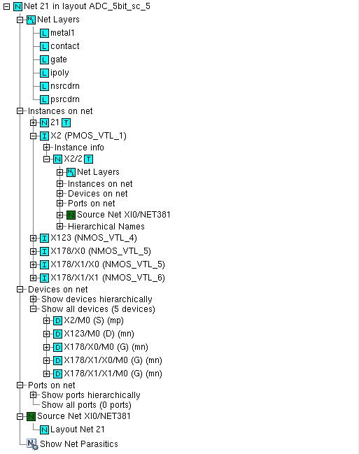
Layer-based views let engineers track how parasitics traverse your entire stack (figure 2), while component-level highlighting pinpoints the exact polygon, segment or via driving parasitic problems.
Filter, sort and correlate instantly
No one’s got time to wade through pages of numbers. Advanced tools let you filter by net, sort by parasitic value, and drill down to specific structures—all linked to physical layout. This type of “click and correlate” workflow slashes debug time, helping teams pinpoint root causes with confidence.
From overview to action: multi-level analysis
A structured, multi-level debugging approach works best:
- Global net analysis: Identify problem nets, signals or regions at the top level.
- Layer interaction review: Examine how each net couples across metal and via layers.
- Component inspection: Zero in on individual polygons or segments.
By narrowing down from the big picture to component details, engineers can resolve issues quickly—often finding tangible fixes among thousands of contributors.
Hit the root cause, not just the symptoms
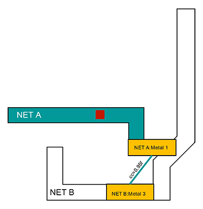
The best IC design visualization isn’t just pretty—it drives action. By explicitly connecting electrical anomalies to their physical layout (figure 3), tools like Calibre make it easy to:
- Highlight problematic segments causing high resistance or capacitance
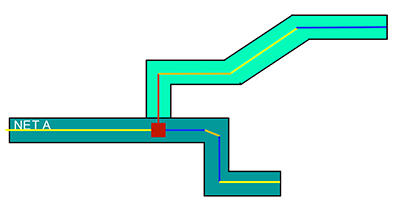
- Run interactive measurements between pins in the layout viewer
- Create automated reports for traceability and compliance, not just for insight
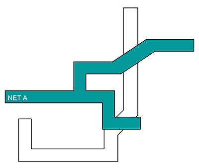
If coupling capacitance between two nets is jeopardizing a SerDes interface, you can modify just one segment to mitigate the issue—instead of rerouting an entire channel. Focused improvements mean faster turnarounds (figure 4).
See the problem, fix the problem: targeted layout modifications
With visualized resistance and capacitance data at your fingertips (figure 5), you can:
- Tweak a narrow trace, add a redundant via or adjust layer assignments
- Quantify exactly how much your fix will improve the design
- Share bookmarks, reports and annotated layouts across your team
Let color guide your focus
Heat maps not only say “where’s the problem?”—they also say, “how bad is it?” You can set sensitivity thresholds to match your specific design needs, ensuring the most critical issues grab your attention (figure 6).
This is especially useful in high-speed I/O blocks, where even moderate coupling can become catastrophic.
Smarter reporting, better collaboration
Today, structured reports go far beyond extraction data dumps (figure 7). Modern workflows deliver:
- Hierarchical and flat net views with device and layer details
- Direct links between extracted parasitics and the physical layout
- Flexible summaries for engineers, managers or compliance teams
Switching between logical and physical perspectives (or between broad overviews and component detail) is a necessity—not a luxury.
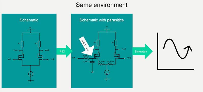
Integrated simulation: no more workflow silos
With tools like Calibre, you can probe schematics, extract parasitics, and launch full simulations—all within a unified environment. This not only accelerates debug cycles, but ensures all teams (circuit, physical, verification) share a “single version of the truth.”
Simulations now fully account for extracted parasitic data. If timing or signal quality is falling short, you’ll see why—and how to fix it—with rapid cycle times (figure 8).
Siemens Calibre: the industry standard for seeing the unseen
All the capabilities above come together in the Siemens Calibre suite: Calibre xRC, Calibre xACT and Calibre xACT 3D for high-precision parasitic extraction, with Calibre Interactive and Calibre RVE providing the visualization and debug experience.
Why do design teams rely on Calibre?
- Up to 50% reduction in parasitic debug cycles
- 35% better first-pass silicon success rates
- 25% gains in critical path timing performance
Calibre delivers not just a unified, graphical environment, but a deeply interconnected workflow: schematic probing, parasitic visualization, heat mapping, simulation and reporting—all in one toolkit.
Custom workflows for every advanced node
Calibre’s framework is flexible. Whether you’re chasing down coupling capacitance in high-speed IO, targeting resistance in power delivery or delving into 3D integration complexities, the environment adapts to your project’s priorities and process technology.
Conclusion: seeing is believing
As we push into ever-smaller nodes and more intricate circuits, hidden parasitics are among the greatest threats to schedule, reliability and product performance. But with advanced visualization environments and structured, interactive debugging, these invisible enemies no longer stand a chance.
With Siemens Calibre, your team gains the clarity, speed and confidence needed for first-pass silicon success—today and across tomorrow’s designs.
Continuing exploring the strategies for tackling hidden parasitic effects in advanced IC design through our full technical paper, “Beyond the netlist: Visualizing the invisible enemies of IC performance,”