IC designers: let’s talk about shift left strategies
By John Ferguson
In the constantly evolving world of electronics, where demands are high for more powerful, efficient, and reliable devices, integrated circuit (IC) design companies face constant pressure to deliver innovative products while reducing time to market. Traditional approaches of throwing more resources at the problem are no longer sustainable. Enter “shift left” strategies, plans, and tools—a game-changer that is gaining popularity in the IC design industry.
Understanding shift left in IC Design
In traditional IC design flows, signoff verification, which includes design rule checking (DRC), layout vs. schematic (LVS) verification, and electrical rule checking (ERC), occurs at the end of the design cycle. It’s a comprehensive process that ensures the design complies with the foundry’s requirements. However, it often leads to a flood of unexpected errors when all components of a system-on-chip are compiled into a single chip. Correcting these errors can be a nightmare, generating multiple rounds of time-consuming debugging and verification iterations.
Shift left involves integrating tasks typically performed at the end of a design process into earlier stages. The primary goal is to catch and correct critical defects and errors at an earlier stage when it’s easier and faster to address them. This strategy not only saves time and resources but also maintains or even improves product quality. To learn more about what a shift left strategy entails, read our technical paper, Shift left with Calibre to optimize IC design flow productivity, design quality, and time to market.
If your company is contemplating a shift left implementation, you may be asking yourself, “How will this affect my role in the design enablement flow? Here are answers to some frequently asked questions to provide you with a clearer understanding of the impact of shift left in IC design.
1. Why should my company consider using shift left strategies?
Shift left strategies offer several compelling advantages, including:
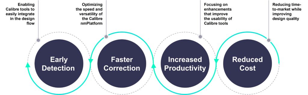
- Time and resource savings: By identifying and resolving issues earlier, you can reduce the number of iterations required, saving valuable time and resources.
- Improved product quality: Addressing defects at an early stage leads to higher-quality designs and reduces the likelihood of critical errors in the final product.
- Efficiency gains: Shift left streamlines the design flow, allowing for smoother collaboration among design teams and faster verification cycles.
- Minimized risk: Easier detection of issues in early stages reduces the risk of costly late-stage design changes.
2. What are the key components of a shift left strategy?
A shift left strategy typically involves the following components:
- Early detection tools: Implement tools and methodologies that enable early detection of design issues, such as DRC and LVS verification.
- Automation: Leverage automation, integration, and user-friendly interfaces to streamline verification processes and reduce manual intervention.
- Collaboration: Foster collaboration among different design teams (e.g., IP designers, block designers, P&R engineers) to address issues collectively.
3. How does shift left affect different IC designers?
- IP designers benefit from shift left strategies in several ways:
- Hard IP: Shift left helps ensure that hard IP components are signoff-clean by spotting changes and fixing errors during the design phase.
- Soft IP: It allows for the early detection and correction of issues in soft IP, such as SRAMs, improving overall design quality.
- Custom IP: Custom cell design becomes more efficient with in-line checking tools, reducing the time and effort required for manual iterations.
- For block designers and P&R engineers, shift left offers the following advantages:
- Early issue identification: It helps identify issues in placements, abstracts, and layouts early in the design process, reducing runtime and error count.
- Efficient ECO handling: Shift left simplifies the handling of engineering change orders (ECOs) by pinpointing changes and enabling targeted checks.
- Custom IP integration: Custom IP cells can be integrated more smoothly, with fewer runtime and error challenges.
- Full chip designers see the benefits of shift left in multiple tasks:
- Focused antenna checks: Shift left narrows down the focus to chip-level nets, simplifying antenna checks and reducing runtime.
- Efficient ECO implementation: Design changes introduced during the final stages become more manageable, reducing the risk of introducing new errors.
- Improved debugging: Identifying changes between design revisions and addressing errors become more straightforward, streamlining the debugging process.
Change can be challenging, but the Calibre shift left solutions are intentionally designed to support the needs of the designers and engineers who use them. To get the full details on how a shift left implementation impacts your role in design enablement, download a copy of our technical paper, What does shift left mean for IC designers?
For even more reading on shift left implementation, visit our Shift left with Calibre solutions webpage, and browse our library of resources.