The path of least resistance…leads to more reliable designs
By Derong Yan
Meeting tapeout schedules and performance requirements are equally critical conditions for IC design success. Now engineers can do both, using innovative P2P resistance checking to find and debug ESD errors in their layouts.
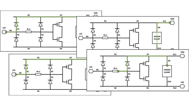
Electrostatic discharge (ESD) is one of the sworn enemies of circuit verification engineers. A single surge of unexpected current can destroy circuitry in a flash (pun intended). Integrated circuit (IC) designers try to build in protection by adding ESD protection devices and discharge paths that direct unwanted current safely away from critical circuitry. However, finding, debugging, and fixing ESD protection circuit errors has always required significant time and resources, and it’s only gotten harder as layouts become larger and more complex. Techniques like visual inspection of layouts just aren’t practical any longer.
But if ESD discharge paths, pull-up/pull-down diodes, and point-to-point (P2P) resistance calculations figure strongly in your nightmares, there’s good news. Electronic design automation (EDA) tools are available that can automate ESD checking to help you quickly identify and fix problematic layouts. For example, the Calibre® PERC™ reliability platform, when combined with the Calibre RVE results viewer and Calibre DESIGNrev™ layout viewer, enables you to not only automatically check the resistances of ESD discharge paths in an IC layout, but also quickly see a visual representation of both the total effective resistance of a path, and the contribution made by each polygon segment to that resistance. This functionality lets you immediately identify the resistance bottlenecks along an ESD path so you can make smart layout changes, such as widening metal routes or adding additional vias, that reduce the total effective resistance of the ESD path to ensure it remains within design limits.
To learn more about ESD resistance violations, and better, faster ways to find and fix them, check out these technical papers:
Checking ESD path resistance in IC designs
Evaluate ESD robustness with cell-based P2P/CD verification
Shortest resistance path deception in ESD protection circuit P2P debug
Debug P2P results using resistance and current density data
Debugging P2P interconnect resistance errors using resistance segmentation
Enhance IC reliability design verification with coordinate-based P2P and CD checking