Tiny Chips, Big Challenges: Full-Chip Electrical Reliability
Need to ensure your chip performs in the real world? The Calibre PERC reliability platform provides fast, accurate, verification for complex reliability issues like ESD, LUP, and TDDB.

By Frank Feng – Mentor, A Siemens Business
Chip designs using advanced technology take advantage of shrinkage in both gate size and interconnect width/spacing to achieve greater functionality in a smaller device. 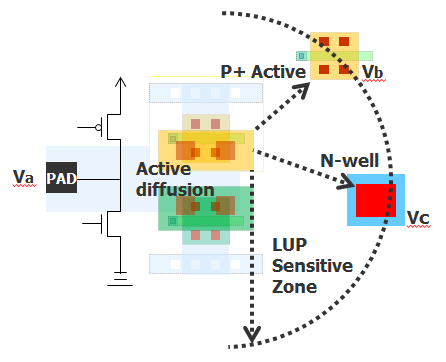 These advanced process nodes enable many more devices to be packed into a die with equal or lesser dimensions than those of a previous node. While process design kits (PDKs) and technology design parameters take into account reliability issues like electrostatic discharge (ESD), latch-up (LUP) and time=dependent dielectric breakdown (TDDB), the post-place and route (P&R) layout still requires full-chip reliability verification to prevent ESD along interconnect paths across multiple function blocks, LUP across gates in the vicinity of IO circuits, and TDDB between interconnects of different nets operated on different potentials. Without such full-chip verification, chip reliability failures become far more likely during the burn-in stage or in silicon.
Using dynamic simulation approaches to analyze ESD, LUP, and TDDB is not feasible for block or whole chip designs, primarily because the large scale of the circuits produces too much data to be processed to provide reliable simulation results in a practical runtime. Employing static design rules is becoming a realistic and effective approach to manage reliability issues in the chip/block-level design stage.
In response to this need, foundries and independent device manufacturers (IDMs) have begun more clearly defining static ESD topology and LDL and LUP/TDDB related voltage aware design rule checking (DRC) checks. Designers can now apply these rule checks to their designs with reliability tools like the Calibre PERC reliability platform to verify the reliability compliance of their designs to foundry and IDM defined ESD/LUP/TDDB rules. With its unique ability to correlate both netlist and layout (GDS) information, in conjunction with static simulation and static voltage propagation, the Calibre PERC platform enables designers to further customize their electrical rule checks that incorporate both circuitry and layout-correlated parameters.
For example, to prevent weak interconnect spots being burned by high ESD current surge, foundries and IDMs define the current density per layer along the ESD path to be smaller than some criteria to survive an ESD event. For ESD prevention, diode/MOS/resistor as ESD or power-clamping device clusters are required to be connected to IO, power, ground, and cross-power domain paths. Calibre PERC platform functionality can trace ESD paths along interconnect to examine current density, and traverse connectivity inside a SPICE netlist to verify that the required ESD dual diodes/power-clamping MOS/back-to-back diodes circuit structures exist or not. Device parameters of all corresponding circuits are also examined to ensure the devices (individual/clustered) have sufficient strength for adequate ESD protection.
For LUP prevention, the rule checks require the use of a delta-voltage-dependent spacing criteria between potential aggressor and victim device layer polygons. Calibre PERC functionality can extract the layout netlist, traverse the connectivity graph, propagate voltage values from IO/power/ground ports into internal circuitry, and locate and export potential aggressor/victim devices annotated with a propagated voltage value. It then generates unique physical layers that correspond to the exported aggressor/victim devices, processes polygon data with annotated properties, and performs spacing DRC checks to find any edges or polygon pairs that violate spacing criteria according to the delta-voltage range.
For interconnect TDDB prevention, the rule checks require spacing checks among polygons of the same interconnect layer on different nets, which are executed against different criteria depending on delta-voltage range. Calibre PERC functionality performs static voltage propagation under a user-constrained propagation scheme, assigns appropriate voltage values to each concerned net, annotates static voltage values to physical polygons of corresponding nets, and runs spacing checks that account for different spacing criteria versus different delta-voltage ranges.
If you’d like to know more about how you can employ static simulation and static voltage propagation in conjunction with logic-driven layout (LDL) analysis for fast, accurate, automated reliability design verification of ESD, LUP, and TDDB issues at the full-chip level, download a copy of our white paper, Full-Chip Electrical Reliability Verification: A New Approach for Advanced Nodes.