Established Technology Nodes: The Most Popular Kid at the Dance
By Michael White, Mentor Graphics
Established nodes have a lot of dancing left to do! Learn how and why new markets are driving new design starts.

I remember back in the day at high school dances, always wanting to dance with the most popular girl in school. I never could, because there were a constant stream of others queued up to dance with her. If you are trying to build an integrated circuit (IC) today, and trying to get fab capacity at 28nm and above, you are faced with the very same situation. Lots of suitors jockeying for access. There are two interesting points to be explored here: 1) why are these nodes experiencing such a long life, and 2) how is this long life driving new challenges for designers?
Why Established Nodes Are Experiencing an Unexpectedly Long Life
The Internet of Things (IoT) means many things to many people, but the segment of IoT related to sensors and connectivity is the answer to the longevity question. The functionality we crave, such as smart power management for longer battery life, and Wi-Fi and Bluetooth for more connectivity, are more cost-effective when implemented at established nodes between 40 nm and 180 nm. Consequently, the high consumer demand for these capabilities is driving increased demand for ICs manufactured using these processes. In a nutshell, the nodes that best support radio frequency (RF) and mixed-signal IC designs with low power, low cost and high reliability are seeing a much higher demand than in the past.
The other dynamic driving a longer than expected life of established nodes—40/45 nm and 32/28 nm in particular—is the wafer cost trend at 20 nm and below. 20 nm and below are well-suited for advanced CPUs, application processors, etc., but from a price/performance perspective, they are generally a poor fit for sensors, connectivity, analog mixed-signal (AMS) applications, etc.
Although you wouldn’t necessarily know it from reading press releases each week, designs at 65 nm and larger still account for approximately 43% of all wafer production and 48% of wafer fab capacity. Even more significant, nodes 65nm and larger account for approximately 85% of all design starts (Figure 1). Clearly, established nodes are not fading away any time soon.
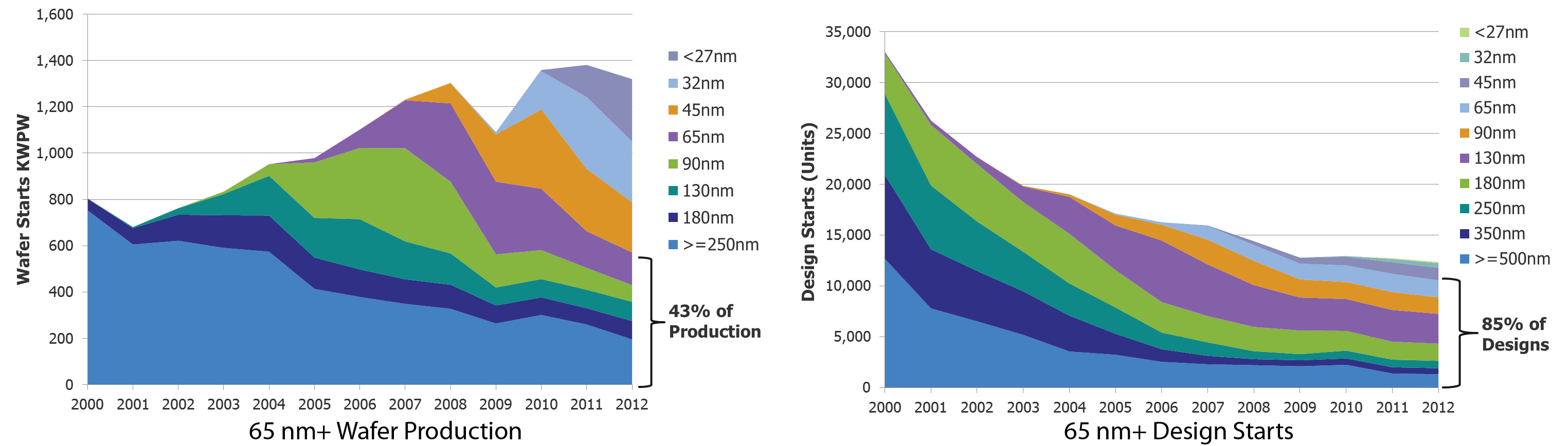
Figure 1. Production data shows established nodes still comprise a significant portion of the IC market. (source: VLSI Research)
Today’s Established Nodes Have Evolved to Meet Market Requirements
Designs at these established nodes are certainly not static. Today’s established node designs are vastly different from the original designs developed when these nodes were new (Figure 2).
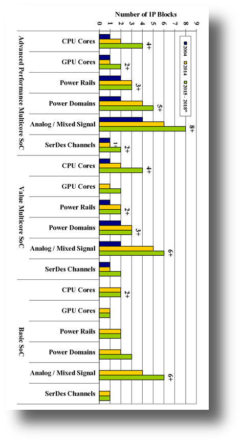
Figure 2. Design complexity at established nodes is increasing, measured here at 65 nm by the number and type of IP blocks in typical designs (Source: Semico Inc.).
Historically, when a node was brought on line, it was optimized for Bulk CMOS digital logic. That is, the process design rules, supported device types, voltages, etc., were all tuned for this application. Today, established process lines such as 65nm are being “retooled” for an assortment of product types (Figure 3). It’s common to see mixed-signal IC designs (e.g., Wi-Fi, Bluetooth, etc.) using process and design rules that never envisioned such products. They require more power, meaning more rails, domains and islands. They contain more analog and mixed-signal components, as well as high-speed interface solutions like silicon photonics. They require a variety of advanced design rule checks (DRC), and “smart” filling routines designed to maximize the use of fill. They often include large intellectual property (IP) blocks, either developed internally or purchased from third-party suppliers. They often have far more reliability constraints, due to new market requirements and standards. And lastly, they are more and more frequently incorporated into a 3D or 2.5D package. All of those changes impact the physical verification strategy and techniques for these designs.
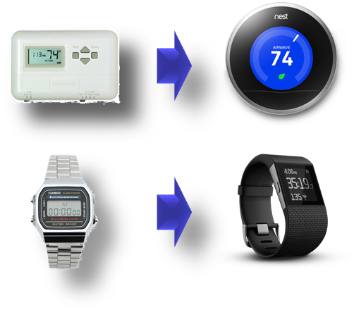
Figure 3. Consumer electronics is one market that powers the relentless drive toward more functionality and sophistication.
Why is this important to you? As a reader of this periodical, you probably work within the IC ecosystem, developing these types of products using an “advanced” mature node. Of course, time to market for a new Wi-Fi or Bluetooth chip built on an advanced mature node is just as important as a 16/14 nm application processor for a next-generation smart phone. And because the design you are building is far more complex than the first designs built on the target process, it may be that your team is struggling, because the EDA tools you used when that process was introduced 5 or 10 years ago cannot handle the new requirements and complexity. Fortunately, electronic design automation (EDA) tools built for later nodes with additional capabilities can be easily redeployed for advanced mature nodes to improve design team productivity and the quality of your designs.
Some of the capabilities commonly employed at advanced mature nodes include:
– Circuit reliability
- Reliability checking to identify design flaws associated with electrostatic discharge protection, electrical overstress, electromigration and others in single- or multi-voltage-domain designs
- Ability to handle voltage-dependent design rules, that is, spacing rules that depend on the voltage potential between devices and wires
- Ability to check for accurate device symmetry in sensitive analog circuits and other reliability-related analog/mixed-signal issues
- Ability to check for reliability conditions that are unique to a particular design methodology
– Pattern matching functionality to identify specific shapes and configurations.
- Ability to define and locate patterns of interest that can affect performance or detract from yield
- Specialty device checking
- Multi-layer structure definition
- SRAM cell, cell interactions, and interface checking
- Ability to detect IP manipulation
– Automated DRC waiver management
- Elimination of time spent debugging waived errors
- Ensure ISO standard compliance for consistent behavior and traceability
– Equation-based design rules, which allow designers to define rules as complex mathematical functions, greatly simplifying rule definition while increasing accuracy.
- Precise tolerance determination on multi-dimensions (such as multi-faceted polygons)
- Accurate antenna checking and property transfer
– Automated fill process that satisfies complex fill requirements
- Maximization of fill shapes to minimize density variation
- Critical-net-aware fill
- Analog-structure-aware fill (symmetry requirements)
- Alternating and symmetrical fill for diffusion and poly
- Matched fill for sensitive devices, cells, nets
Naturally, EDA vendors are stepping up to the challenge, and working to ensure these capabilities are available to design companies working at established nodes. At Mentor, we see extensive use of the tools in our integrated Calibre® nmPlatform being used for verification across the circuit and physical layout domains. Designers and foundries see that leading-edge tools such as the Calibre PERC™ reliability solution, the Calibre eqDRC™ functionality of Calibre nmDRC™, the Calibre Pattern Matching tool, SmartFill™ functionality in Calibre YieldEnhancer™, and others can provide as much value to the established nodes as they have for the newest processes.
Summary
The latest IC design and verification challenges are not all at the latest and greatest process node. Competition and market demand continue to challenge designers working at established nodes as well. In addition, industry economics and specialized applications are creating a growing volume demand for designs based on established nodes. While the market potential of established nodes is growing, so is the complexity and difficulty of validating designs that push these nodes far beyond their original capabilities. The new reality is challenging designers using EDA tools that were not available when the nodes were brand new. We’re learning that EDA tools are not frozen to the node, but must advance at these advanced established nodes just as they do at the leading-edge nodes. Design teams working at advanced established nodes have the option to upgrade their tools and make their life much easier. They might even feel like dancing…
Author
Michael White is the Director of Product Marketing for Calibre Physical Verification products at Mentor Graphics in Wilsonville, OR.

Liked this article? Then try this –
White Paper: Is Complexity Increasing For Designs Done at Older Process Geometries?
This article was originally published on www.semimd.com