MEMS Technology and Manufacturing on the Microscale
By Carey Robertson and Khaled AbouZeid, Mentor Graphics
Designers incorporating MEMS devices into high-volume CMOS ICs need new processes, data, and tools from foundries and EDA vendors

When you turn your tablet sideways, and the display automatically repositions itself, do you ever stop to think about what made that happen? Microelectromechanical systems (MEMS) are micro-scaled mechanisms designed for two primary applications:
- Sensing—changes in sound, motion, pressure, and temperature. Sensing can include not just physical movement, but also vibration, acoustic waves, fluid waves, light waves, heat, and air pressure.
- Actuating—conversion and management of light projection/reception, radio frequency signal processing, and fluid management. Actuation can include detection, filtering, conversion, and modulation.
The size of a MEMS device typically ranges from 20 micrometers to a millimeter, while the size of MEMS sub-components is in the range of 1 to 100 micrometers. MEMS functionality has been incorporated across a wide range of industrial and consumer markets, such as automobile safety and control systems, smartphones, tablets, video game controllers, drug delivery, microphones, gas and chemical sensors, and much, much more. These markets are continuing to grow as new innovations and applications emerge (Figure 1).
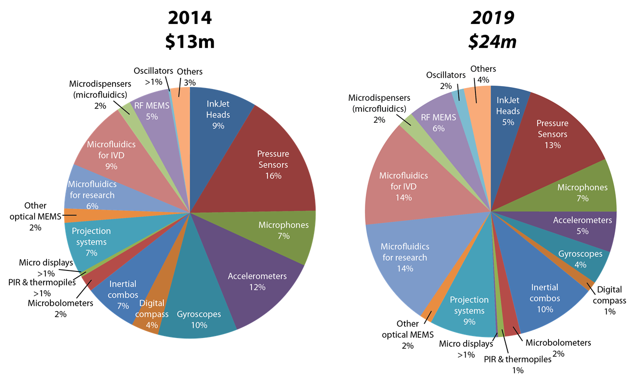
Figure 1. The MEMS market is predicted to grow substantially over the next few years. (Source: image courtesy of Yole Developpement)
In place of traditional integrated circuit (IC) components like transistors, resistors, and diodes, MEMS mechanisms contain highly calibrated physical structures such as springs, screws, gears, and plates (Figure 2). MEMS devices also use different types of processing. To achieve the physical dimensions, techniques such as surface micro-machining, bulk micro-machining, deep reactive ion etching (DRIE), and molding are required.
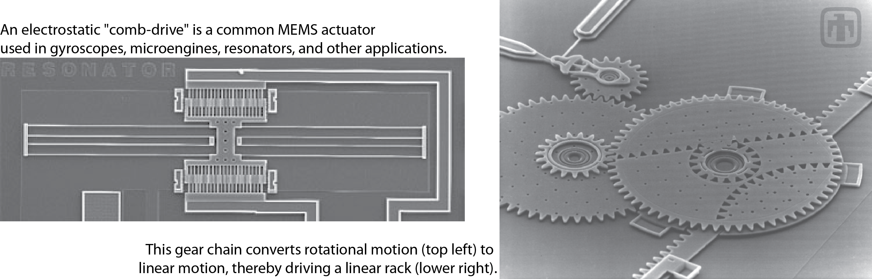
Figure 2. MEMS devices
Historically, MEMS devices have been manufactured using highly-specialized processes that are customized for each device type. This wide assortment of MEMS fabrication processes results in higher market production costs and a longer time to market schedule. As the market moves towards the integration of MEMS devices into high-volume CMOS IC manufacturing, the MEMS technology faces the challenge of shortening development time, reducing costs, and meeting increasingly complex performance and reliability requirements. Incorporating MEMS design directly into the CMOS design flow offers the best chance to achieve these goals, but what elements are needed to make this integration happen?
- Component library. A MEMS component library contains proven physical parameterized primitives that are fabrication-ready. Designers can select primitives and define parameters (length, radius, thickness, etc.) to instantiate a component in the layout. The library is also used to supply these material properties to subsequent simulations.
- Design tool. An effective MEMS design tool must provide a graphical user interface to enable designers to initiate instantiation, create new blocks, connect components, and add application-specific structures and modifications. This same tool should also provide a layout view to display the MEMS design and generate 3D views.
- Process simulation tool. This tool models the results of the actual process flow based upon process settings and physical simulation of the process, such as diffusion, growth, or etching, all of which are unique to the target foundry and manufacturing line. It is similar in nature to IC lithography simulation tools. Designers use this tool to conduct simulations using multi-physics simulators, which conduct simultaneous simulations of the device in different domains (e.g., mechanical and electrical). They can also refine device behavioral models, and identify and correct design errors before test fabrication. These simulations help designers understand the effect of the process on the final physical geometry of the MEMS device. However, since they are based on actual physical models, they are often very time-consuming.
- Productivity tools. This category includes automatic layout generation tools that take abstract MEMS system descriptions as input and generate detailed multi-component physical layouts, as well as macro model generators, which convert detailed physical verification results into compact models for analysis and system-level verification.
Linear, iterative design flows can quickly become a time sink for a MEMS design team. Structured design flows that efficiently exchange information between the schematics, process flows, layout, 3D finite element analysis (FEA) and boundary element analysis (BEA), and package analysis can allow the MEMS designer to exchange information with process, design, electronics, packaging, integration, and software engineers.
Verification of MEMS devices also requires somewhat of a departure from traditional IC design verification. The IC world typically uses layout vs. schematic (LVS) comparison and design rule checking (DRC) techniques for physical verification. Just like traditional ICs, DRC is a necessary step for MEMS devices to validate that a particular design can be manufactured in the targeted process. However, the structures encountered in a MEMS design can differ dramatically from traditional circuits. A typical MEMS design will have curved geometries, Bézier curves, and a variety of all-angled layouts. Fortunately, by using advanced physical verification technologies like equation-based DRC, rules can be written that accurately describe real design errors by translating the curves into a gridded structure like GDSII.
LVS is a different paradigm, due to the inherent 3D nature of the design. Many MEMS designers go right to physical implementation and do not develop a “schematic.” Therefore, one of the main functions of LVS, which is to compare the schematic against the layout, is not required. However, the first action of LVS is to “extract” the layout and develop a device and connectivity model of the entire design. This step requires the LVS tool to recognize the complex 3D structures that exist in the design, and differentiate those from the structures, wires, etc. that connect the devices to each other, to electrical sensors, and to the outside world. This electrical and connectivity model is necessary for MEMS verification because it enables other downstream functions, such as parasitic extraction (PEX), and ultimately, circuit simulation. By leveraging the capabilities of new reliability verification tools that can link together the ability to perform circuit classification, physical layout measurements, complex calculations, and rule-driven circuit checking, the specific curvatures of the devices and interconnects can be verified against the designer’s intent.
Speaking of PEX, simulating MEMS device behavior reveals another verification challenge. Traditional PEX tools are rule-based or table-based methodologies, and are developed with certain assumptions about the physical layout. These tools are developed to support the interconnect that exists in IC designs; therefore, they are optimized for rectilinear geometries and parallel and orthogonal routes. These assumptions fail when the PEX tool encounters the complex geometries found in MEMS designs. MEMS circuits require the type of accuracy that is only available from a field solver. Advanced extraction solutions that combine true field solver technology with the performance and scaling of modern parasitic extraction tools must be used if designers want to achieve the verification accuracy required for these MEMS circuits while maintaining targeted tape-out cycles.
Testing requirements also differ considerably. Traditional ICs typically use a single generic tester for most electrical tests. MEMS devices normally require a series of tests, which can include physical stimuli such as mechanical shock, variable frequency vibration testing, and temperature cycling. Standard qualification tests such as high and low temperature operating life ensure long-term reliability.
Foundries must provide standardized MEMS processes, and collaborate with fabless MEMS design houses, to meet time-to-market and high-volume production demands. Designers also need process design kits, MEMS IP libraries, and reference flows from foundries. Test engineers need to incorporate appropriate environmental tests. In short, the changing MEMS market calls for nothing less than a new silicon and software ecosystem—much of it based on the fabless model familiar to IC design companies—to enable designers to turn out products for the cost-driven, high-volume consumer market.
By integrating the power of mechanical and optical functions with silicon, MEMS devices can add significant functionality without the need for transistor scaling. However, the success of integrated chips will depend in large part on the ability of the industry to ensure reliable, cost-efficient products can be produced in high volume in a timely manner. That goal, in turn, depends on the ability of the foundries and EDA vendors to provide the designers with the processes, data, and tools they need to create integrated ICs that combine the advantages of MEMS and silicon circuitry to satisfy the growing market demand.
Authors
Carey Robertson is a Director of product marketing at Mentor Graphics Corp., overseeing the marketing activities for Calibre PERC, LVS and extraction products.
Khaled AbouZeid is a technical marketing engineer in the Design-to-Silicon division of Mentor Graphics Corp., focusing on Calibre parasitic extraction technologies and MEMS EDA solutions.

Liked this article? Then try this –

This article was originally published on www.eetimes.com