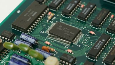
Manufacturing Driven Design leverages the intelligence within your PCB Design

Intelligent Process-Driven DFM Analysis for PCB Designers
Recent component shortages and distribution disruptions have exposed both the fragility of global supply chains, as well as underlined the benefits of linking intelligent data systems throughout a product’s lifecycle. Small to medium-sized businesses unable to leverage vertical integration solutions have been increasingly adopting supply chain-wide intelligent integration solutions. This end-to-end intelligence adoption follows the lifecycle of a product and its digital twin, straight from an adaptive approved vendor list (AVL) with a robust part library, to final production runs.
Design for Manufacturing (DFM) solutions must also apply intelligent data use within the PCB design process. Intelligent DFM allows product specifications to merge seamlessly with manufacturing capabilities, allowing data to drive decisions in a process known as Manufacturing Driven Design. Making use of a true digital twin for your product’s lifecycle is reliant on leveraging the intelligent systems already in place and is vital to maximizing production efficiencies through process automation.
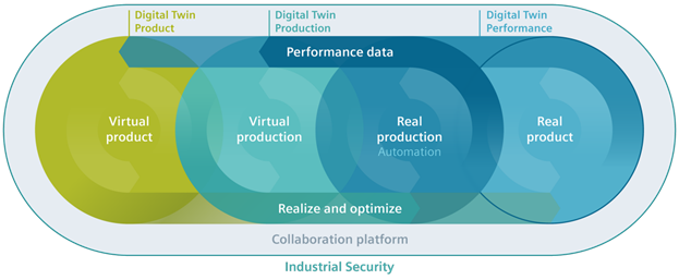
A Digital twin ties together all phases of the manufacturing process, from design to shop floor operations. For a PCB designer the performance data is produced from a series of DFM product offerings that provide various automated board simulations and which communicate seamlessly across multiple platforms via an intelligent data format; from dielectric material selection and PCB stackup design simulation, through to PCB Signal Integrity (SI) and Power Integrity (PI) simulation, to PCB manufacturing simulation.
Automating Intelligent DFM in 3 steps
Automating intelligent DFM not only helps to streamline efficiencies into the entire production process and to ultimately work to produce a product of higher quality at lower costs, but it also allows for more consistent results between unique products and across designers.
For a PCB designer, the digital simulation manifests as a 3-step process that identifies opportunities to optimize a PCB design. This is based on factors, classifications and constraints and represents a true start-to-finish digital twin simulation that leverages data from across the supply chain. Information gathered from fabrication, assembly, and test is used to inform design decisions to facilitate each step. Factors such as copper weight, layer position or layer technology can be used to provide precise process limits for many layer-specific factors. These requirements can be identified from intelligent data systems and then automatically passed to process-based DFM to generate intelligent and actionable analysis results.
Step 1: Gather PCB Design Factors
The first step in DFM automation is gathering all the known design factors present within your board. A design factor is a characteristic of the board that drives the initial analysis decision. The information and intelligence of the design factor has been derived from the attributes and properties in the CAD data.
When manufacturing a rigid-flex board, intelligent DFM software, such as Siemens’ Valor NPI automatically interrogates the design file and checks to see if a copper layer with the subtype identified as ‘flex’ is present. If the board contains flex layers it will enable a series of flex-specific DFM checks. Within an intelligent data system, these values are determined via dataset interrogation – in most cases, they exist with ODB++ attributes or are calculated values.
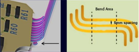
Due to the delicate materials used, flex and rigid-flex designs are more likely to incur damage during the manufacturing process, causing them to produce naturally lower yields. This makes specific checks to transition area and flex regions a necessary addition to ensure manufacturability.
One such example would be on the conductor spacing between the rigid board and the bend region of a flex circuit. Generally, 5mm is the accepted distance between the board and bend region for a flex circuit to allow for an adequate bend radius.
By applying DFM analysis to flexible PCB design, communicating this global manufacturing knowledge into your design factors, DFM software like Valor NPI can automatically resolve this calculation and flag this issue during the design process, presenting it as an opportunity to increase yield.
Classification Factors
A classification factor, like the example of rigid flex above, defines PCB design types based on a production process requirement and the board characteristics. They can be thought of as a precondition test on your product model. This could include things like the layer count or the presence of specific technologies such as Microvias, Rigid-flex or HDI. The classification factors present here go on to determine the design classification that will be applied to the DFM analysis.
Constraint Factors
A constraint factor represents a threshold value that is applied to a board characteristic. This could be represented by copper weight, a drill size, or any calculated value which forces a class decision, like trace width and spacing.
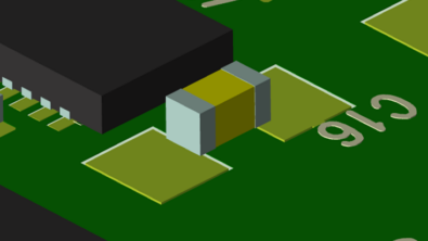
An area factor is a type of constraint factor that represents the different naming conventions provided to individual areas of a board based off DRC areas or assembly process areas. These may include press-fit areas, reflow areas, or any number of other conditions. The area factors are either keep out or keep in and derive their naming condition from their respective analysis configuration parameters. An example of this is having a different spacing constraint for features underneath a BGA than for the rest of the PCB .
The determination of these constraints depends on knowledge of your suppliers’ manufacturing capabilities. These constraint values are used to fine tune your analysis and come into play in step 3 of the automation process.
Step 2: Generate PCB Design Classifications
The classifications portion of intelligent, automated DFM is a series of generated thresholds used to query against the determined design factors within your board. The thresholds are perhaps based on IPC Class levels, or maybe on the capabilities of your suppliers. Updating your automated DFM to accommodate for new technology can be as simple as updating the values within your design classifications. Based on the classifications you have created; the intelligent DFM system will automatically choose the lowest threshold classification that satisfies all the requirements.
Step 3: Apply PCB Manufacturing Constraints
Manufacturing process constraints are created using design restraints as well as information about the identified board type. These constraints are passed through an analysis to generate results. The generated constraints are the method used to determine how the board is analyzed in order to assess the quality of the design from a manufacturing point of view.
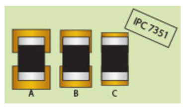
IPC-7351 Density Level represents generic requirements for surface mount design and the land pattern geometry variation developed to accommodate wave or flow solder for leadless chip devices. IPC-7351 allows for 3 levels of constraint factors (Most/Nominal/Least) based on the calculated footprint allowance. These density levels generally conform to the rotational tolerances present on a PCB assembler’s pick-and-place machine.
The determination of these three levels within your validation will depend upon the reliability of your libraries and the knowledge of your suppliers manufacturing capabilities. Having a robust bi-directional data transfer system is vital in the identification process
Constraints are grouped related to a specific analysis action and can be separated into six general categories
- Etch – Bare board manufacturing issues that are etch related, including copper spacing, annular rings, and drill to copper. These are located exclusively in signal layers, power and ground layers, and mixed layers.
- Mechanical – Bare board and assembly issues resulting from physical tooling like microvias and backdrilling.
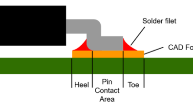
- Solder – Assembly issues related to soldermask and silkscreen as well as pin and pad connections.
- Quality – Assembly and fabrication issues that affect the testability or physical appearance of the board.
- Process Setup – Process issues that affect assembly.
- Component Placement – Assembly issues that affect the ability to place or inspect components on boards or panels.
Automated DFM Analysis
The analysis gathered from this 3-step process presents a comprehensive simulation of your design relative to the manufacturing capabilities communicated to you by your contract manufacturer (CM) or fabricator. In this way, your supplier’s digital process twin can provide you feedback concurrently with the design process, without the need for a physical re-spin.
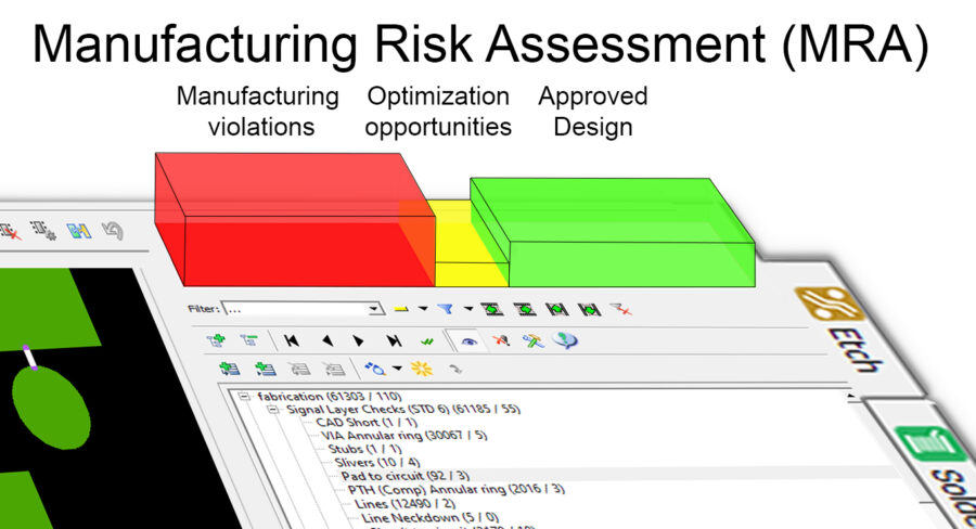
Valor NPI’s Manufacturing Risk Assessment (MRA) tool presents your PCB’s performance data coupled in constraint groups and sorted based on a simple 3-tiered color system:
Red – Violations will occur making manufacturing impossible.
Yellow – The product will be manufacturable but will have reduced yield.
Green – Design elements are optimized.
It is the intelligence in the design data and the DFM software that enables the automated DFM analysis, making the benefits of DFM of use to more people. This intelligent and automated DFM process is designed to integrate seamlessly into your workflow regardless of the EDA tool you use and leverages the information already present across that workflow to create more reliable and lower cost products.
Signup today for a free online trial of Valor NPI for Xpedition, or any other EDA flow.