Design today, reuse tomorrow: mastering IP management for electronics teams
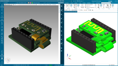
PCB design complexity now exceeds what point tools and disconnected handoffs can manage well. Fragmented workflows separate design intent from implementation, creating manual work, avoidable errors and respins.
High-performing electronics teams do not just move faster through layout. They reduce risk earlier by asking a better question: can we build it?
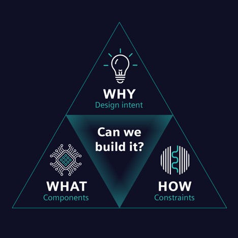
That question changes everything. It shifts Intellectual Property (IP) management from a file-reuse exercise into a strategy for preserving design intent, improving manufacturability, and accelerating new product introduction. It also matters financially. Lifecycle Insights’ study, An Analysis of the Impact of PCB Design Practices on Performance, reinforces the value of integrating manufacturability insight directly into the PCB design workflow. The study found that PCB designs average 2.9 respins before reaching volume production, with each rework cycle adding roughly two weeks and more than$28K in material costs alone. It also showed that teams using integrated DFM tools complete 49% more designs annually and improve time-to-market by 12%.
For lean engineering teams, the stakes are even higher. Generalist engineers often wear multiple hats. They spend too much time on manual schematic entry, component research, documentation, and data validation instead of high-value engineering work. That is why modern IP management must go beyond storing reusable files. It must connect reusable design assets, supply chain intelligence, verification, and manufacturing readiness in one scalable workflow.
What IP management means in electronics design
In electronics development, IP is any reusable engineering asset that helps a team design faster and with more confidence.
Common forms of reusable IP
- Library assets: symbols, footprints, 3D models, parametric data, manufacturer part numbers (MPN), supplier part numbers (SPN) and form, fit, and function (FFF) approved alternates
- Circuit and layout assets: schematics, PCB layout blocks, variants, reference designs
- Design intent: constraints, stackups, placement rules, exception rationale, design requirements
- Verification assets: ERC/DRC configurations, SI/PI setups, DFM profiles, validation checklists
- Process assets: release packages, review templates, manufacturing outputs, documentation standards
If a team cannot clearly identify what is approved for reuse, it is not practicing governed reuse. It relies on “tribal knowledge” and institutional memory.
Why informal reuse fails as designs scale
Most electronics teams begin with ad hoc reuse. An engineer copies a prior design, updates the schematic, swaps a few parts, and pushes ahead. That approach works until complexity rises.
Common failure modes of informal reuse
- Constraints are reused without the original rationale.
- Libraries drift across teams and product lines.
- Approved parts become obsolete or risky without visibility.
- Documentation is recreated manually from disconnected data.
- Production issues appear late because manufacturability was not checked early.
These failures are expensive because they hide in plain sight. A design may appear complete, but the underlying intent is fragmented across emails, spreadsheets, local libraries, and tribal knowledge.
The real cost of disconnected workflows
Systems and PCB design complexity has outgrown “throw it over the wall” workflows. Schematic capture, layout, component selection, verification, DFM review, and documentation cannot operate as isolated tasks if the goal is first-pass success.
This is especially visible in new product introduction. PCB documentation remains one of the largest sources of manual effort in NPI.
The flow of design intent
- Converting requirements into manufacturing-ready specifications
- Validating disconnected design data across tools and stakeholders
- Manually generating drawings and release outputs
These are not just documentation problems. They are evidence that design intent is not flowing cleanly through the development process.
Documentation also creates a structural challenge. It takes significant engineering time yet contributes little visible value to the finished product in the eyes of the end customer. As a result, documentation is often deprioritized or treated as a final administrative task. That is a mistake. Poor documentation increases manufacturing complexity, creating inconsistency between builds and undermines product quality.
Documentation should not be a disconnected end step. It should be the natural output of a connected design process.
The teams that win optimize digital prototypes
The best practice is simple: optimize digital prototypes before release. At Siemens, we call these optimized digital protypes comprehensive digital twins: a complete, validated representation of your design before it goes to production.
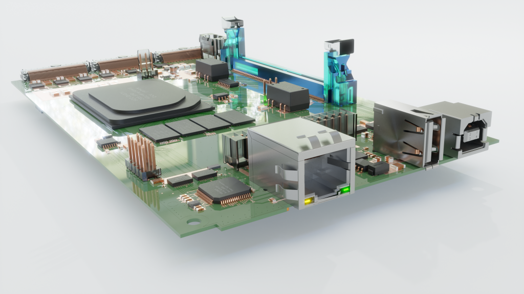
That means verifying not only whether the circuit works, but whether the design can be manufactured efficiently, documented accurately, sourced reliably, and handed off without ambiguity.
A robust digital prototype preserves:
- design intent
- implementation details
- component intelligence
- verification status
- manufacturing constraints
- documentation readiness
When teams optimize digital prototypes, they reduce manual translation between stages. They also reduce the gap between what was designed and what can actually be built.
Five best practices for mastering IP management
1. Digitize design intent
Reusable IP should capture more than geometry and connectivity. It should preserve the reason behind engineering decisions.
What to standardize
- Constraint templates by product class
- Approved exceptions with rationale
- Reusable circuit blocks with design context
- Stackup strategies and placement guidance
- Requirement-to-implementation traceability
When design intent is digitized, reuse becomes safer and verification becomes more consistent.
2. Empower component and library intelligence
A library is not just a storage location. It is a controlled engineering resource.
What strong library governance includes
- A single source of truth for symbols, footprints, and 3D models
- Release states such as draft, reviewed, released, and deprecated
- Approved manufacturer and vendor strategies
- Lifecycle status and supply chain risk visibility
- Library audit trails and ownership
This reduces part-related escapes and gives teams more confidence during design reuse.
3. Eliminate design data siloes
Disconnected tools force engineers to manually reconcile intent, implementation, and outputs. That is slow and error-prone.
Connected design data should link
- schematic to layout
- component to sourcing data
- design intent to constraints
- ECAD to manufacturing requirements
- released design data to documentation outputs
When data continuity improves, teams spend less time validating files and more time improving design quality.
4. Verify and validate continuously
Verification should happen throughout the design process, not only at the end.
Reusable verification IP can include
- ERC and DRC templates
- SI and PI setup templates
- DFM rule profiles
- standard signoff checklists
- traceable waivers and approval workflows
This is where the question “can we build it?” becomes operational. Manufacturability becomes part of design, not an afterthought.
5. Optimize digital prototypes for manufacturability and resilience
This is the key update for today’s PCB teams. Digital prototypes should be continuously improved against manufacturing, sourcing, and documentation requirements before release.
What this looks like in practice
- Actionable DFM insights inside the design workflow
- Early visibility into part risk and alternates
- Automated documentation generated from connected design data
- Manufacturing outputs that reflect actual design intent
- Fewer manual handoffs between engineering and production teams
The business case is strong. Teams that integrate DFM into their workflow complete more designs annually and reach market faster. More importantly, they avoid sinking time and material cost into preventable respins.
A practical maturity model for IP management
Use this model to benchmark your current state.
| Maturity level | Characteristics | Typical risk |
| Ad hoc | Files on shared drives, reuse by memory | Unknown provenance |
| Organized | Naming rules, partial library control | Inconsistent reuse quality |
| Governed | Approvals, versioning, release workflows | Limited cross-domain continuity |
| Connected | ECAD, supply chain, collaboration, manufacturing workflows aligned | Better traceability, fewer siloes |
| Optimized | Metrics, automation, continuous verification, digital prototype optimization | Highest resilience and scale |
Most growing electronics teams sit between organized and governed. That is where a more connected approach can deliver outsized gains.
What modern tooling should enable
Electronics teams need more than standalone authoring tools. They need an environment that supports reuse, collaboration, and buildability across the full flow.
Look for these capabilities
- governed reusable blocks and libraries
- release and revision control
- integrated supply chain intelligence
- collaboration and markup without data duplication
- DFM insight during design
- automated documentation and manufacturing outputs
- scalability from individual users to multi-team environments
This is where a connected ecosystem approach becomes valuable. Siemens positions the Xpedition product family as a scalable electronic systems design ecosystem that supports teams from independent engineers to global enterprises. The advantage is data and process continuity across design domains. Teams can start with the level of capability they need, then expand without retraining users or translating data between unrelated tools.
For growing teams, Xpedition Standard provides advanced PCB design capabilities with a balance of cost-efficiency and scalability. For engineers looking for professional-grade PCB design at an entry-level price, PADS Pro Essentials offers access to Xpedition technology in a streamlined starting point. The principle is straightforward: start where you need, scale when you’re ready.
What to measure
If reuse is working, performance should improve in measurable ways.
Useful IP management KPIs
- reuse ratio for released blocks and libraries
- time-to-first layout
- time-to-release
- number of respins per project
- library-related error escape rate
- percentage of parts with approved Form-Fit-Function (FFF) alternates
- documentation cycle time
- late-stage ECO volume
- DFM issue discovery timing
These metrics help teams move from anecdotal improvement to operational improvement.
Connecting design intent to implementation
IP management is no longer just about reusing past designs. It is about preserving design intent, reducing manual work, and ensuring that what is designed can actually be built.
The teams that perform best do not treat manufacturability, verification, and documentation as downstream tasks. They optimize digital prototypes continuously. They connect design data across the workflow. They reduce respins by making buildability visible earlier.
That is how electronics teams design today and reuse tomorrow.
Start a 30-day trial.
Watch the webinar: Accelerate PCB design productivity with AI and intelligent automation
Frequently asked questions about PCB IP management
What is IP management in PCB design?
IP management in PCB design is the practice of organizing, governing, and reusing design assets such as schematics, layout blocks, libraries, constraints, and verification templates.
Why do PCB respins happen?
PCB respins often happen because of manufacturability issues, poor communication of design intent, disconnected workflows, and late discovery of sourcing or documentation problems.
What is a digital prototype in electronics design?
A digital prototype is the combined representation of a product’s design intent, implementation, verification status, and manufacturing readiness before release to production.