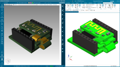
Facilitating design reuse and IP management in PCB design: Transforming engineering knowledge into a scalable competitive advantage

Moving beyond reinvention
As PCB and electronic system complexity continues to accelerate, engineering organizations are under constant pressure to deliver faster development cycles, higher quality products, and greater innovation while operating with tighter schedules and constrained resources. Yet despite significant advances in PCB design technologies, many organizations still rely on fragmented workflows, tribal knowledge, and highly manual development methodologies that force engineers to repeatedly solve problems that have already been solved. This constant reinvention creates massive inefficiencies across the enterprise.
Valuable engineering knowledge often becomes trapped within completed projects, unmanaged libraries, or individual expertise rather than being transformed into reusable organizational intelligence. Engineering teams repeatedly recreate circuitry, rebuild constraints, redefine routing methodologies, and duplicate verification effort instead of leveraging proven solutions that already exist within the organization.
The traditional design-from-scratch methodology is no longer scalable. As electronic systems become increasingly complex, organizations can no longer depend solely on individual expertise and informal reuse practices to achieve predictable success. Engineering knowledge must evolve from isolated project output into reusable enterprise intelligence.
Organizations that successfully facilitate design reuse and IP management understand this shift clearly. They recognize that engineering knowledge is one of the company’s most valuable strategic assets and that capturing, validating, managing, and scaling that knowledge can significantly improve engineering efficiency, product quality, and long-term competitiveness.
Design reuse is no longer simply an engineering convenience. It has become a business strategy.
The growing challenge of PCB design complexity
Modern PCB development has evolved far beyond traditional board layout practices. Today’s electronic systems integrate high-speed serial interfaces, dense HDI and UHDI structures, complex power delivery networks, multi-domain constraints, and increasingly demanding performance requirements within shrinking form factors.
At the same time, organizations are expected to deliver products faster while maintaining reliability, manufacturability, and regulatory compliance. This growing complexity is exposing the limitations of legacy development methodologies.
In many organizations, engineering success still depends heavily on the experience of individual designers rather than standardized and scalable engineering processes. While engineering expertise remains invaluable, relying on tribal knowledge as a primary development strategy introduces significant operational risk.
The result is repeated design effort, inconsistent implementation methodologies, extended verification cycles, avoidable design respins, and reduced engineering scalability. As organizations expand globally and support distributed development teams, these inefficiencies become even more difficult to sustain.
Engineering organizations cannot continue solving modern complexity challenges with disconnected workflows and ad hoc reuse methodologies. The companies scaling successfully today understand a critical reality: reusable engineering intelligence is now essential for sustainable product development.
What effective design reuse really means
Design reuse is often misunderstood as simply copying circuitry from previous projects. In reality, modern reuse strategies are far more strategic and far more valuable.
Effective reuse involves systematic capture, validation, management, and deployment of proven engineering knowledge across the organization. This includes reusable circuit blocks, validated subsystem architectures, standardized constraints, routing methodologies, stackup definitions, floorplanning strategies, and verification workflows.
Constraint reuse represents one of the most overlooked opportunities for improving engineering consistency and accelerating development. Organizations can standardize differential pair rules, impedance requirements, return path management strategies, crosstalk mitigation methodologies, and manufacturability constraints rather than rebuilding them for every project. This is where engineering organizations begin transitioning from manual implementation toward scalable engineering methodologies.
Equally important is preserving design intent. One of the biggest weaknesses in many reuse initiatives is that organizations preserve the design data but fail to preserve the engineering reasoning behind it. Successful reuse strategies capture not only what was designed, but why specific decisions were made. This includes performance tradeoffs, manufacturing considerations, reliability objectives, simulation results, and system-level constraints.
Without preserving intent, organizations risk reusing designs incorrectly or losing valuable engineering knowledge over time. When properly implemented, design reuse enables engineering teams to leverage validated knowledge with greater confidence, consistency, predictability, and scalability.
Why IP management matters
Design reuse cannot succeed without effective IP management. Many organizations already possess enormous amounts of valuable engineering IP but lack the infrastructure, governance, and standardization required to manage it effectively. As a result, reusable content often becomes fragmented, outdated, difficult to locate, or inconsistently validated. When engineers lose confidence in reusable assets, they revert to recreating existing work. That is where engineering inefficiency quietly compounds.
Modern IP management strategies focus on transforming reusable engineering data into trusted enterprise assets. This requires centralized repositories, version control, qualification processes, metadata classification, lifecycle management, and secure access control.
Validated reusable IP should include supporting documentation, revision history, performance limitations, simulation data, and manufacturing considerations. Reusable content must be trusted before it can be effectively scaled across the organization.
As development ecosystems become increasingly distributed and collaborative, protecting and managing engineering IP also becomes essential for maintaining long-term competitive advantage.
The business value of design reuse
Organizations that successfully implement reuse and IP management strategies often realize benefits that extend far beyond engineering productivity. One of the most immediate advantages is accelerated time-to-market. By leveraging validated design assets, engineering teams can reduce redundant effort, minimize rework, shorten verification cycles, and improve development predictability.
Reusable and validated IP also improves product quality. Proven design blocks, standardized methodologies, and reusable constraints reduce variability and engineering uncertainty, helping organizations lower defect rates, reduce respins, and improve manufacturability.
Design reuse additionally improves engineering scalability. Standardized methodologies make onboarding engineers easier, support geographically distributed teams, and reduce dependency on tribal knowledge. This creates more resilient and adaptable engineering organizations.
Perhaps most importantly, reuse enables highly skilled engineers to focus on innovation rather than repeatedly solving foundational implementation challenges. Design reuse is not about limiting innovation. It is about eliminating unnecessary reinvention. Instead of repeatedly rebuilding existing architectures and workflows, engineering teams can allocate more time toward system optimization, advanced technologies, and product differentiation.
Collectively, these improvements contribute to lower development costs, improved engineering throughput, stronger profitability, and better return on R&D investment.
Best practices for facilitating design reuse and IP management
Organizations seeking to modernize PCB development workflows should approach reuse as a strategic transformation initiative, rather than simply a tooling enhancement.
Successful reuse initiatives begin with standardization. Consistent naming conventions, constraint methodologies, verification processes, documentation practices, and design governance create the foundation for scalable and trustworthy reuse.
Hierarchical and modular design approaches also play a critical role. Modular architectures allow organizations to encapsulate reusable functions, simplify integration, improve maintainability, and accelerate future product development.
Equally important is the creation of validated reuse libraries containing approved components, reusable circuit blocks, standardized constraints, stackup profiles, and reference architectures. These libraries should be continuously maintained and governed to ensure long-term reliability and engineering confidence.
Organizations should also integrate simulation and verification directly into reuse workflows. Reusable content should include signal integrity analysis, power integrity validation, thermal analysis, and manufacturing verification whenever possible. Validated reusable IP dramatically reduces downstream engineering risk.
Cross-domain collaboration is another essential component of successful reuse strategies. Modern PCB development requires alignment between electrical, mechanical, manufacturing, thermal, and reliability disciplines. Reusable IP should reflect these interconnected requirements rather than isolated design perspectives.
Automation and intelligent design technologies will also continue reshaping how organizations implement reuse methodologies. Constraint-driven workflows, reusable templates, AI-assisted optimization, and integrated data management platforms are enabling engineering teams to scale best practices more consistently than ever before.
Finally, executive-level sponsorship is essential. Organizations that treat reuse and IP management as isolated engineering initiatives often struggle to achieve meaningful adoption. Companies that successfully scale reuse recognize it as a strategic business initiative directly tied to engineering efficiency, product quality, operational scalability, and long-term competitiveness.
Reuse as a strategic engineering imperative
Facilitating design reuse and IP management is no longer optional for organizations developing increasingly complex electronic systems. In today’s competitive environment, organizations must move beyond isolated project-centric development methodologies and begin treating engineering knowledge as reusable enterprise intelligence. Engineering organizations that continue relying primarily on tribal knowledge, disconnected workflows, and manual reinvention will face increasing difficulty scaling product development efficiently and predictably.
Companies that successfully implement modern reuse strategies achieve faster innovation cycles, improved product quality, greater engineering scalability, reduced operational risk, and stronger long-term profitability. More importantly, they empower engineering teams to focus less on repetitive implementation tasks and more on delivering innovation that drives meaningful business value.
The future of PCB design will not be defined solely by how quickly organizations can create new designs. It will be defined by how effectively they can capture, manage, reuse, and scale engineering intelligence across the enterprise. That is where true engineering transformation begins.