Busbars Save The Day! And Your Favorite Electronic Devices Too
Busbars carry significant amounts of current with harmonics at relatively high frequencies. They are the unsung hero in power distribution equipment and power inverters. However that can create electromagnetic noise and interfere with the performance of nearby devices. Only by performing an electromagnetic analysis of busbars can you get the complete picture and avoid product failure and damage.
Power Inverters & High Powered Emissions
A power inverter converts direct current (DC) to alternating current (AC) at a specified voltage and frequency to operate and control devices such as variable speed AC motors. This level of control is made possible by very fast turn-on and turn-off by semiconductor devices. One such device is an Insulated Gate Bipolar Transistor (IGBT). Ideally, the output voltage waveform of such a device should be sinusoidal. However, in practice, the waveforms contain harmonics at much higher frequencies. This makes the inverter one of the major sources of electromagnetic interference (EMI) in Electric Vehicles (EVs) and Hybrid Electric Vehicles (HEVs). Electromagnetic noise from the parasitic effects can be anywhere from 1 to 15 MHz.
Today’s IGBTs can handle substantial currents and are very fast at switching currents demanded by modern-day applications. However, this also means that the conducted and radiated emissions carry much more power. High powered emissions can potentially damage connected devices and other devices in the vicinity if not dealt with appropriately. An example of problems that could be caused by electromagnetic emissions are:
- false control signals
- errors in sensors
- electromagnetic noise causing fidelity issues
- damage or other adverse effects on the performance of other electronic devices
The harmonics content of the output voltage of the power semiconductor devices are significantly reduced by switching techniques. However, optimizing the other components in the inverter will help maintain a low overall inductance to mitigate EMI issues. Consequently, the design and optimization of the busbar connecting the switches to all the other components become critical.
The Critical Role of Busbars
Busbars are the backbone for power applications. They provide the critical interfaces between the power module and the rest of the system. In many applications, there is a requirement to conduct substantial amounts of current. Additionally, there is a requirement for components to become smaller, faster, and more complex. To meet these challenging requirements and performance specifications, busbars are continually redesigned.
Since busbars are made of solid copper or aluminum, there is significant current redistribution due to the high-frequency content in the waveform. This makes it essential to take into account the skin and proximity effects during the optimization process. Additional constraints should also be taken into account. One such constraint is the current density levels to prevent overheating in any part of the device. Another is maintaining a balanced current at the output terminals, and an accurate evaluation of the current distribution is required.
The image below represents the busbar structure of a power electronics application. In most cases, the busbar structures are detailed and complex.
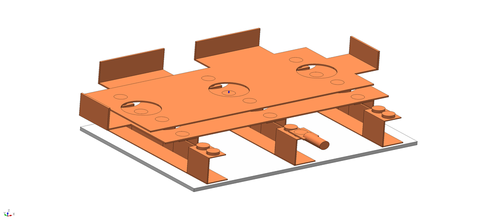
Busbar system of an IGBT inverter
The challenge with modeling busbars, in particular for many of the power electronics devices, such as inverters, is that they form a complex network of coils linked to IGBTs, diodes, capacitors, and so on. This makes the requirement for circuit modeling different from other applications when it comes to the electromagnetic analysis of busbars.
With the new addition to the circuit modeling in Simcenter MAGNET 2020.1, we have overcome the modeling obstacle by allowing the insertion of a circuit component anywhere inside a busbar and including it in the finite element field simulation domain.
New Circuit Capability for Electromagnetic Analysis of Busbars
As shown in the figure below, with the new circuit capability, a gap is created where the user can insert an electric circuit component. In this example, a switch and a diode are inserted.
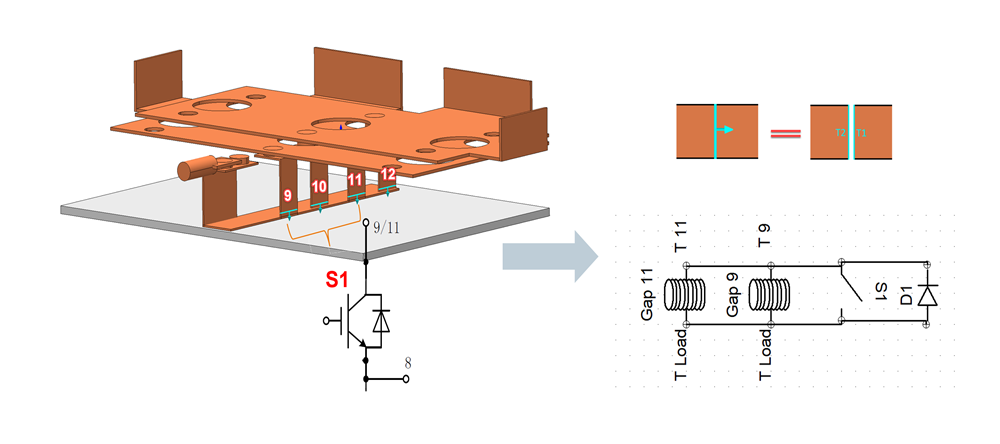
Electric circuit components inserted in the busbar gaps
The above figure shows an IGBT inverter, where four gaps are created to insert the switch. The switches are sandwiched between the copper layers, which form the electromagnetic computation domain.
Electromagnetic Analysis of Busbars: Transient Simulation
With this new capability, the designer can perform one transient simulation and obtain all the distributed field quantities. This includes the ability to take skin and proximity effects into account.
It is possible to instantly evaluate the current distribution in the busbar to detect any hot spots due to geometric constraints and skin and proximity effects.
The stray inductance of the busbar system is accurately computed and lowered through optimization to mitigate EMI issues. Additionally, the current and voltage waveforms at the terminals for very fine time steps are readily available for inspection.
Having the complete time-domain distributed field results helps in multi-physics simulations, such as temperature rise, to optimize for lowest heat dissipation, and so much more. As can be seen in the current density plots, skin effects, and proximity effects are all taken into account in one simulation run.
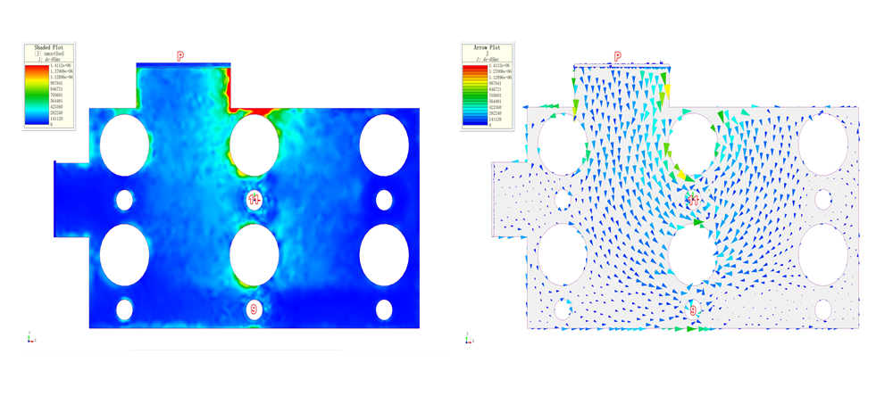
Current distribution in the bottom layer
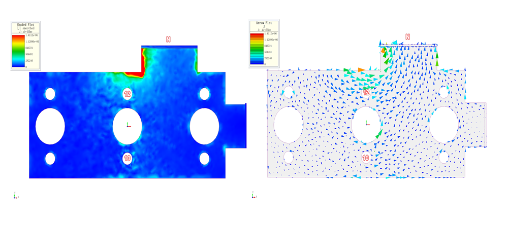
Current distribution in the top layer
As we can see, the current density plots show the asymmetrical parallel branches of the busbar.
Here are some results for the double pulse test for verifying the IGBT over-voltage and stray inductance of the busbar with just one transient run.
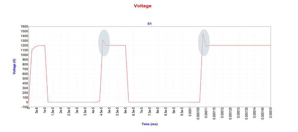
The spike in the voltage waveform due to the busbar’s stray inductance
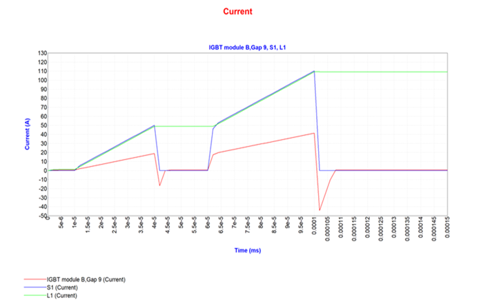
The load current, the current of the switch, and the current of one branch of the busbar
Preventing EMI issues at an early stage through simulation is crucial to avoid costly additions of other components and hardware at a later stage to correct the problems. The 3D electromagnetic analysis of busbars using advanced circuit modeling inside the electromagnetic field computation domain plays a significant role in this respect.


