The smart path to STCO with Hierarchical Device Planning (HDP)

The heterogeneous integration of multiple chiplets in a single packaging platform is critical for many high performance compute segments such as AI, Hyperscalers, HPC, Cloud datacenters, Neural processors and even autonomous vehicles. This increased design complexity requires the use of a System Technology Co-Optimization design methodology which leverages iterative multi-physics analysis during the floorplanning stage and optimization of the chiplets, the interposers and the package substrate to achieve PPA and cost goals, significantly lowering the barrier for project success. Trying to employ traditional chiplet, interposer and substrate design approaches – where each device is modeled as a single flat entity – is time consuming and unnecessarily risks delaying production and yielding an un-optimized overall result. Siemens partnered with Intel Foundry to develop a STCO centric capability that enables a “smart path” to homogeneous disaggregation using Hierarchical Device Planning and parameterized pin regions.
The path to chiplet architectures
Significant resources are dedicated to advanced semiconductor bump planning, interposer/substrate pathfinding/floorplanning and overall device assembly. Today’s designs are typically assembled from various forms of design data including Verilog netlists, LEF/DEF and bump maps in spreadsheet form. Once assembled, design teams can begin system technology co-optimization (STCO), which entails interactively optimizing the interfaces on the IC or ICs as well as the target PCB. The rise of graphical floor planning tools with advanced connectivity management, like Innovator3D IC Integrator (i3DI) from Siemens EDA, has made this possible.
In this blog we will discuss an efficient methodology for homogenous disaggregation. It starts with a semiconductor package floorplanning/pathfinding environment such as Innovator3D IC Integrator that enables fast design updates. This allows us to utilize block-level implementation process to create and update hierarchical blocks. For this blog I will discuss how a design comprising of a single SoC flanked by 4 HBM memory stacks, two on each side.
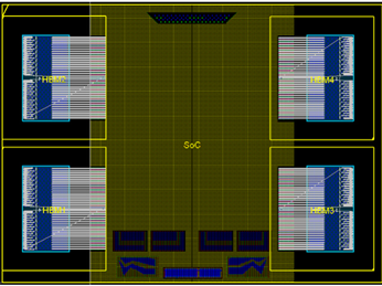
I will provide insight into an efficient and effective methodology/process that will allow the designer to disaggregate the existing SoC into four for cost effective chiplets, such as this:
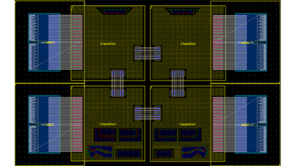
When disaggregating an SoC into chiplets design iterations become a major driver for the use of hierarchical device planning. Design structures that are comprised of hierarchical building blocks can be updated quickly when a change is required in one of the referenced blocks.. In contrast, design updates using non-graphical IC package floorplanning/pathfinding process rely on macro driven spreadsheets to generate bump maps can be time consuming and error-prone.
The key benefit of using hierarchy is clear – a large and complex design can be disaggregated into smaller and easier to manage building blocks based on collection attributes such as function and position. To find out more about this process I urge you to read this excellent white paper by Chris Cone The smart path to chiplets | Siemens Software who also presented this methodology and process at IMAPS-DPC and Chiplet Summit conferences.