3D of a PCB

PCB high voltage spacing: What every engineer should know

At the heart of high-voltage PCB reliability is proper PCB high voltage spacing between conductive elements.

Aerial view of agricultural silos.

Beyond silos: Enabling multidomain and multidiscipline integration in electronic systems design

Engineering success depends not just on deep expertise, but on seamless integration across domains and disciplines.

Icons of file folders

Design for manufacturing output files – optimizing engineering to manufacturing efficiency

As PCB design and manufacturing become increasingly complex, the choice of design for manufacturing output files plays a crucial role in streamlining processes, reducing errors, and improving time to market.

blind and buried vias

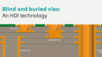
Blind and buried vias: An HDI technology

One of the key innovations within HDI PCB design is the use of blind and buried vias, which enhance routing capabilities by freeing up additional routing resources, increasing the amount of routing channels while requiring fewer signal layers, and optimizing board space.

Optimizing FPGA/PCB co-design: Best practices and industry insights

Previously on episode 20 of the Printed Circuit Podcast, host Steph Chavez explored the intricacies of FPGA (field-programmable gate array)…

Breaking down silos: the future of electronical-electronic co-design in cable and harness engineering

In a recent episode of the Printed Circuit Podcast, host Steph Chavez sat down with Erica Van Berkum, a leader…

A person working on a PC design using Xpedition

Things to check for on a PCB

What stage a PCB, or a PCB assembly (PCBA) is in determines what things to check for on a PCB.

Abstract close-up of the Microchip on green circuit board

Where to put decoupling capacitors on a PCB: best practices and design considerations

Why where to put decoupling capacitors on a PCB can make or break your design.

Two women working together at a white board,

Concurrent design: revolutionizing PCB development

Concurrent design minimizes errors and project delays in PCB development.