The Importance of a Quality PCB Stackup
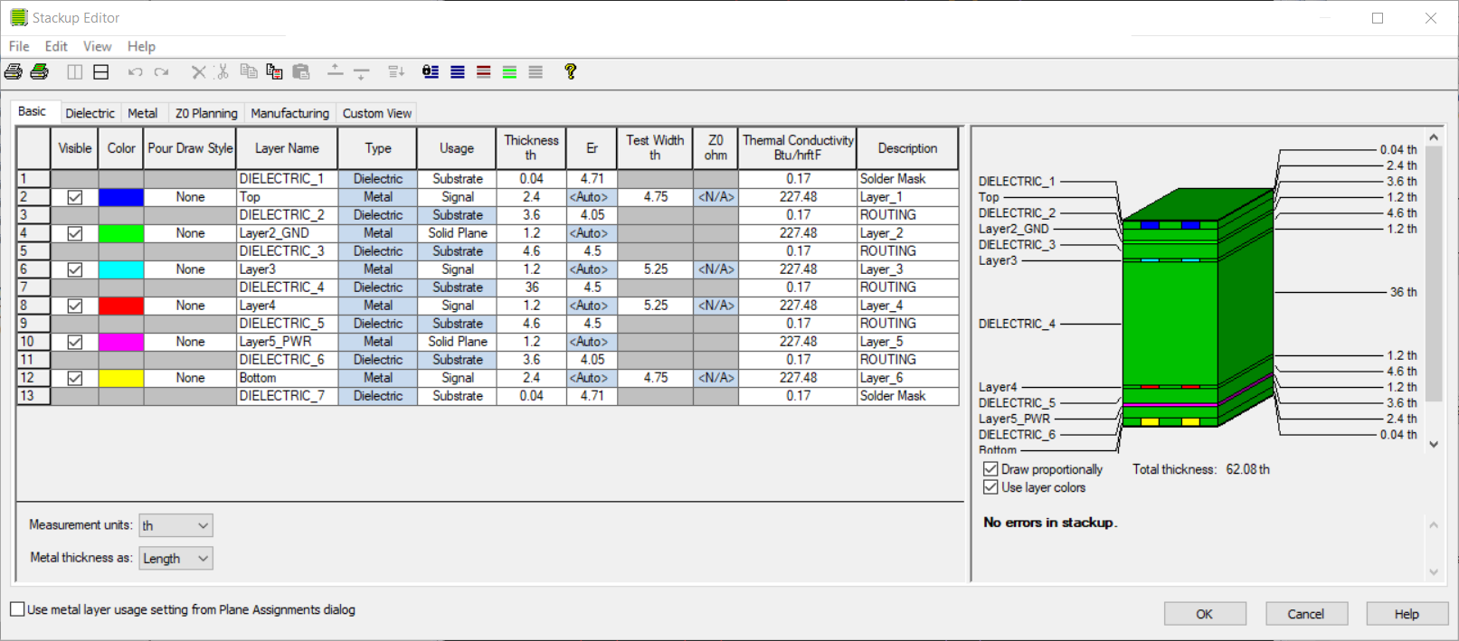
Stackups, as minor as they may seem, can make or break a PCB design. With the latest technology incorporating ICs with edge rates well below the nanosecond range, a well planned stackup is as important as ever. When defining your board’s stackup, there are electrical factors, layer substrates, and costs to consider.
Electrical factors:
In designing any circuit, trace parameters effect the signal integrity, crosstalk, and electromagnetic interference of your design. We’re living in a world where high speed designs with different technologies is the norm – creating a necessity for finely designed stackups accommodating trace widths and impedance variations to meet design requirements.
Substrates:
Variations in layer arrangement and material in a stackup can prove to cause very different final crosstalk and signal integrity results. For example, deciding to use power planes in multi-layer stackups can aid in shorter return paths and temperature control throughout the board.
Costs:
Costs vary from project to project – based on materials used and layers in your stackup. It’s important to work with your NPI team and fabricator to make sure you’re using materials that are both cost efficient in meeting your design requirements. Looking into heights of different dielectrics, whether or not to add a power plane, number of ground planes, etc. can be beneficial to the design and reduce costs – it all comes down to requirements and restrictions.
If you want to learn more about PCB stackups, check out this video for tips. To learn more about avoiding crosstalk and signal integrity issues, we have a webinar that would be worth diving into. Enjoy and happy designing!
Thanks for reading,
Shivani