Did I build that right? Testing in high mix, low volume PCB production
With the shift to high mix PCB assembly, there are more new product introductions (NPIs) to process and debug. How are test engineers managing this increase in workload that leaves little time for test strategy with fewer test engineers? What does this mean for test plan management?
Now that high-mix, low-volume production is the new norm, the old tried and true testing methods no longer offer a scalable solution.
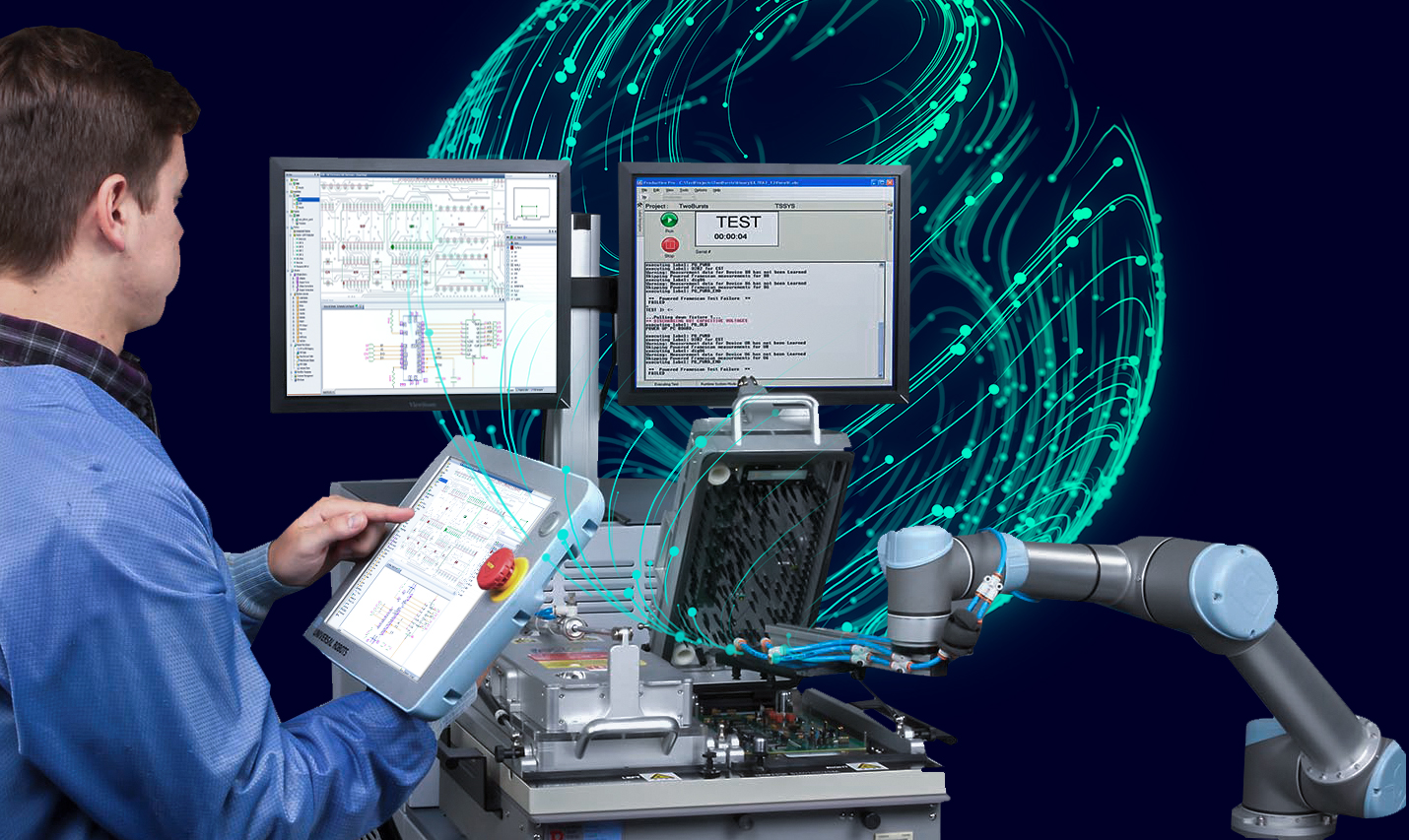
Doing more PCB testing with fewer resources
Between process verification and product verification, testing engineers check that the product is built correctly and will work to design specification. Challenges that electronics manufacturers face today with high mix PCB production revolve around scalability. How can test engineers possibly keep up using traditional testing methodologies? Simply put – they can’t keep doing what they’ve always done.
With multiple data preparation applications, each using different source files, and the need for comprehensive PCB functional testing and process validation, there is simply no way test engineering departments can create reliable, debugged programs fast enough to meet the dynamic demand.
PCB production test engineering evolution alongside market needs
To meet the needs of the market, shift focus from what test engineers did in the last decade to understanding and anticipating needs for the next ten years. Testing plans focusing on scalability that matches the market needs will result in repeatable test management plans. Versatility in testing capabilities is also an important factor as users will need to do multiple tasks.
A single point of truth in PCB testing
New solutions are needed to enable automated PCB testing. For example, data needs to include all test attributes, and the probe placement needs to create output that machine software can use to finalize test programs. Manufacturers also need a single application for all steps in the line. A digital twin provides a single point of truth for each specific product and is key to mitigating the PCB board testing challenges of high-mix production.
Importance of accurate design data for PCB test engineering
One example of leveraging digital twin data to decrease manual testing is leveraging accurate design data. With design data, test engineers do not need to determine access manually. Analysis software can understand copper, masks, and drill features and automatically determine which are accessible (or not).
To learn more about how to create more efficient testing solutions, register now for the on-demand webinar: Test Engineering in Today’s High Mix Electronics Manufacturing World.