What is Design for Manufacturing?
January 4, 2022
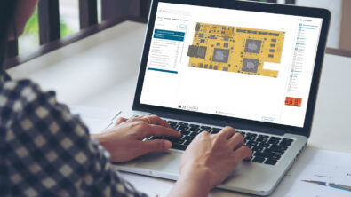
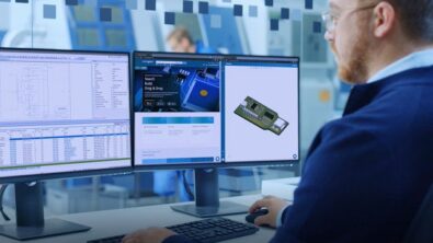
PCB Design for Manufacturing DFM looks at all factors that may impact the manufacturability of a PCB design, such as assembly, fabrication, flex/rigid-flex, microvia, panel and substrate. It should also consider whether SMT component placement and soldering can be conducted automatically to reduce costs. DFM can involve general manufacturing specifications and/or the specifications of a specific manufacturer.