Unmanufacturable via structures you may not know in a design

Vias in a design
Vias, which are small holes drilled through the Printed Circuit Board (PCB) layers, facilitate connections between different layers, they allow signals to travel across the board. Improperly designed vias can lead to fabrication challenges, resulting in unnecessary back-and-forth communication between designers and PCB fabricators. This not only wastes your time but is also completely avoidable.
When an unmanufacturable via structure is sent to your fabricator, your design may be rejected by the fabricator and re-design the via structure is needed, re-routing the complex HDI area that impacted by the via structure may take several hours or a day which is really annoying and frustrating.
Via types
Vias come in various types, each type is suited for a specific design need and are impacted by factors like board density, thickness, and cost. Here are the main types of vias used in PCB design:
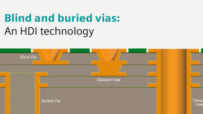
- Through-hole vias: The most common type of via, it extends through the entire PCB.
- Buried vias: Vias connect between two inner layers of the PCB without penetrating to the outer layer.
- Blind vias: These connect an outer layer of the PCB to an inner layer, but do not penetrate through the entire PCB

Common via concerns you may know
There are some general guidelines to consider when designing your via structure. These should be widely known across the industry and are likely present within your general company design guidelines, or are noted within IPC standards.
- Aspect Ratio: The aspect ratio is the ratio of the board’s thickness to the via’s diameter. A high aspect ratio can cause plating challenges, potentially leading to weakened via structures that are improperly plated.
- Blind and Buried Vias: Designing blind and buried vias should be symmetrical in Z-axis, if not, the asymmetrical structure will cause warpage and reliability issue to the final manufactured board.
- Via-in-pad Technology: Via-in-pad places vias directly on the component pads, reducing space and improving signal integrity for a design. However, via-in-pad designs require the vias to be filled and planarized to ensure proper component soldering and prevent solder flowing into the vias. Without proper filling and planarization, issues during assembly can occur.
- Stacked Vias: Stacked vias involve multiple blind vias stacked vertically over each other. It saves space on your board, but, these structures can be prone to reliability problems.
Unmanufacturable via structures you may not know
Besides the common via design practices, there are still some uncommon via structures that can cause the vias to be unmanufacturable in a PCB fabrication process.
Here are some examples of unmanufacturable via structures:
- Overlapping blind and buried vias: Layers connected using a blind or buried via can form a subassembly, the subassemblies is typically laminated together using prepreg layers, so, the overlapped subassemblies are seen as an illegal via definition and unmanufacturable structure.

- Bind and buried vias should not span an odd # of copper layers: When the blind and buried via spans an odd # of copper layers, it forms an asymmetrical structure. Asymmetrical via structures can induce uneven thermal expansion and contraction during manufacturing processes, leading to warpage and twist.

- Blind and buried vias should not have the same start and stop layer: Another unmanufacturable problem for blind and buried vias is they have the same start and stop layer. The via subassemblies(blind via and buried via in this example) should not share the same start and stop layer, this causes no drill access point for one of the subassemblies.

- Blind and buried via span cannot be manufactured as an individual subassembly: If the via structure cannot be broken into individual subassemblies, it becomes unmanufacturable, in the example below, even if it was possible, the top layer will see five plating steps, which is an extremely challenging task for a PCB laminate. Considering using a back drill to achieve the structure below as a preferred practice.

Conclusion
Understanding the characteristics of manufacturable via structures is important for successful PCB design and fabrication. By following solid DFM guidelines and consulting your fabricators, designers can prevent unmanufacturable boards, reduce costs, and accelerate the development of reliable electronic products.
To ensure the manufacturability of your stackup, Siemens provides a dedicated tool to perfect the vias and stackup design process, which helps you to avoid the risk of generating an unmanufacturable via structures and save your time in the design to manufacturing releasing cycle.